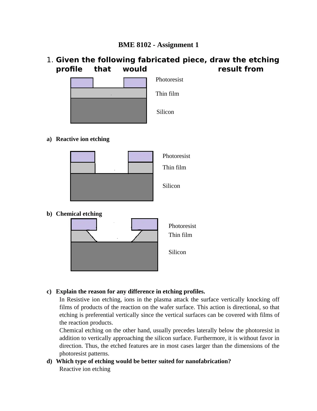
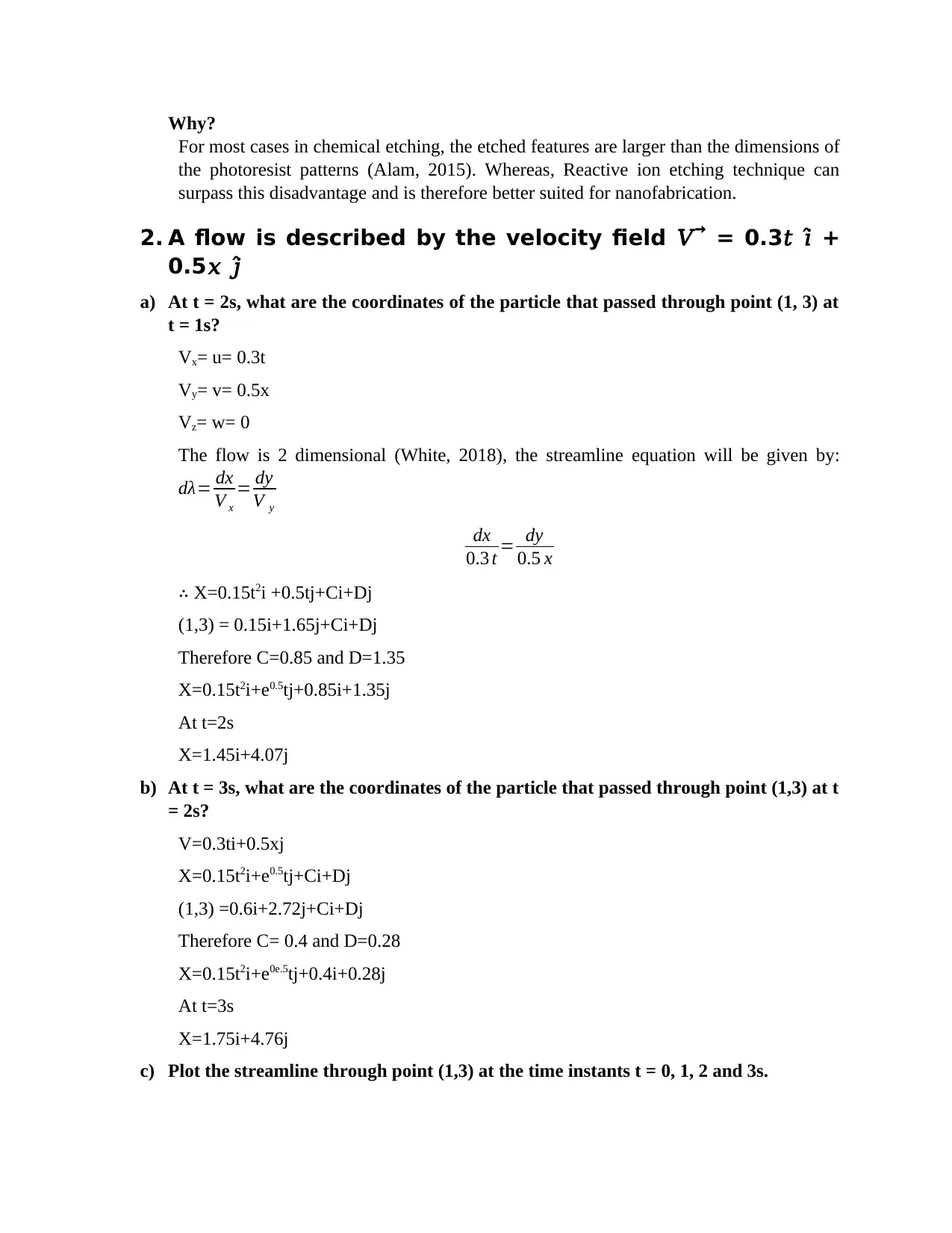
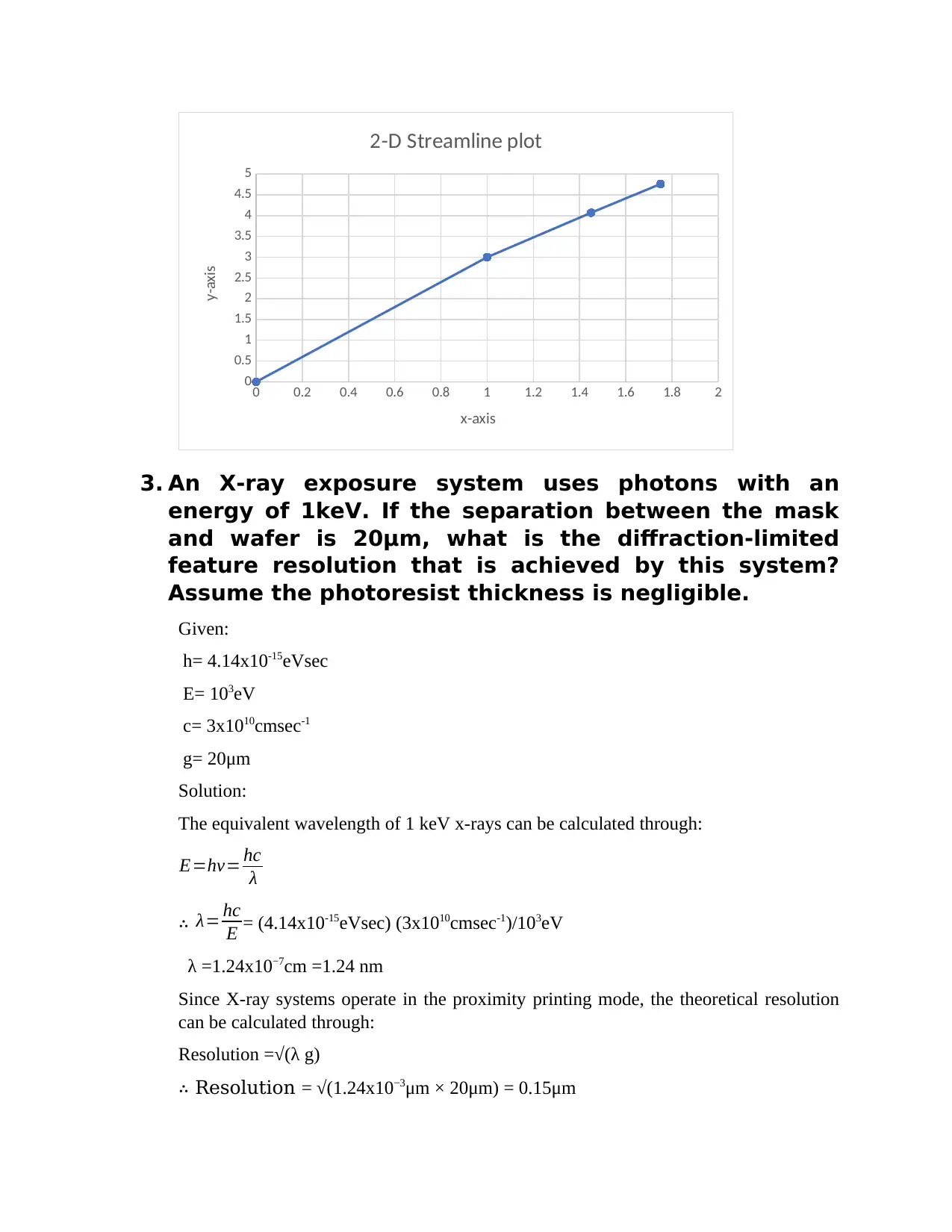
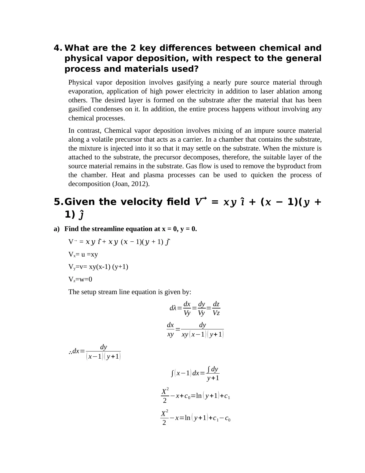
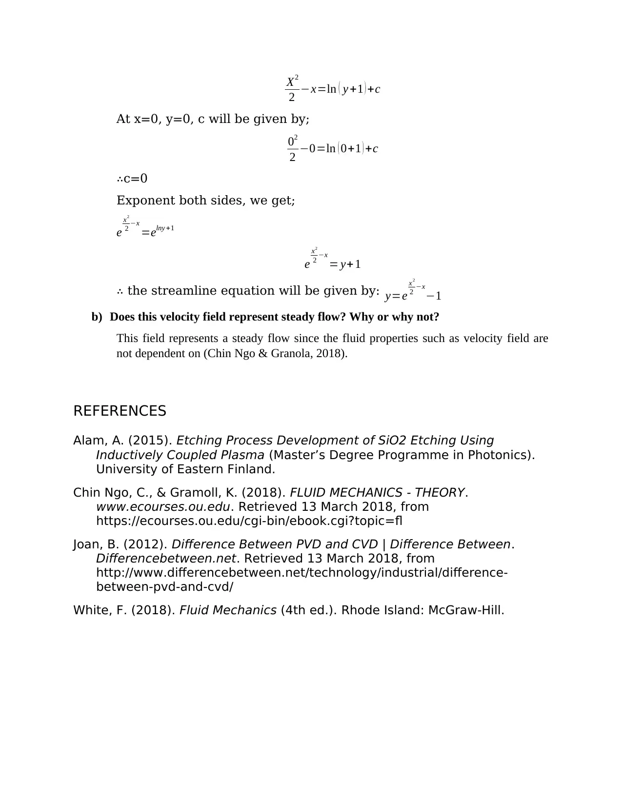
BME 8102 - Assignment 1: Exploring Etching, Flow, and Vapor Deposition
VerifiedAdded on 2023/06/15
|5
|1076
|411
Homework Assignment
AI Summary
This assignment solution for BME 8102 delves into several key areas, beginning with an analysis of etching profiles resulting from reactive ion etching and chemical etching, highlighting the differences in their mechanisms and suitability for nanofabrication. It then explores fluid dynamics, calculating particle coordinates at different time points within a given velocity field and plotting streamlines. The assignment further investigates X-ray exposure systems, determining the diffraction-limited feature resolution. Finally, it contrasts chemical and physical vapor deposition processes, emphasizing differences in materials and procedures. Desklib offers this and other solved assignments to aid students in their studies.

BME 8102 - Assignment 1
1. Given the following fabricated piece, draw the etching
profile that would result from
a) Reactive ion etching
b) Chemical etching
c) Explain the reason for any difference in etching profiles.
In Resistive ion etching, ions in the plasma attack the surface vertically knocking off
films of products of the reaction on the wafer surface. This action is directional, so that
etching is preferential vertically since the vertical surfaces can be covered with films of
the reaction products.
Chemical etching on the other hand, usually precedes laterally below the photoresist in
addition to vertically approaching the silicon surface. Furthermore, it is without favor in
direction. Thus, the etched features are in most cases larger than the dimensions of the
photoresist patterns.
d) Which type of etching would be better suited for nanofabrication?
Reactive ion etching
Photoresist
Thin film
Silicon
Photoresist
Thin film
Silicon
Photoresist
Thin film
Silicon
Paraphrase This Document
Need a fresh take? Get an instant paraphrase of this document with our AI Paraphraser

Why?
For most cases in chemical etching, the etched features are larger than the dimensions of
the photoresist patterns (Alam, 2015). Whereas, Reactive ion etching technique can
surpass this disadvantage and is therefore better suited for nanofabrication.
2. A flow is described by the velocity field 𝑉 ⃗ = 0.3𝑡 𝑖̂ +
0.5𝑥 𝑗̂
a) At t = 2s, what are the coordinates of the particle that passed through point (1, 3) at
t = 1s?
Vx= u= 0.3t
Vy= v= 0.5x
Vz= w= 0
The flow is 2 dimensional (White, 2018), the streamline equation will be given by:
dλ= dx
V x
= dy
V y
dx
0.3 t = dy
0.5 x
∴ X=0.15t2i +0.5tj+Ci+Dj
(1,3) = 0.15i+1.65j+Ci+Dj
Therefore C=0.85 and D=1.35
X=0.15t2i+e0.5tj+0.85i+1.35j
At t=2s
X=1.45i+4.07j
b) At t = 3s, what are the coordinates of the particle that passed through point (1,3) at t
= 2s?
V=0.3ti+0.5xj
X=0.15t2i+e0.5tj+Ci+Dj
(1,3) =0.6i+2.72j+Ci+Dj
Therefore C= 0.4 and D=0.28
X=0.15t2i+e0e.5tj+0.4i+0.28j
At t=3s
X=1.75i+4.76j
c) Plot the streamline through point (1,3) at the time instants t = 0, 1, 2 and 3s.

0 0.2 0.4 0.6 0.8 1 1.2 1.4 1.6 1.8 2
0
0.5
1
1.5
2
2.5
3
3.5
4
4.5
5
2-D Streamline plot
x-axis
y-axis
3. An X-ray exposure system uses photons with an
energy of 1keV. If the separation between the mask
and wafer is 20μm, what is the diffraction-limited
feature resolution that is achieved by this system?
Assume the photoresist thickness is negligible.
Given:
h= 4.14x10⁻¹⁵eVsec
E= 103eV
c= 3x10¹⁰cmsec-1
g= 20μm
Solution:
The equivalent wavelength of 1 keV x-rays can be calculated through:
E=hν= hc
λ
∴ λ= hc
E = (4.14x10⁻¹⁵eVsec) (3x10¹⁰cmsec-1)/103eV
λ =1.24x10⁻⁷cm =1.24 nm
Since X-ray systems operate in the proximity printing mode, the theoretical resolution
can be calculated through:
Resolution =√(λ g)
∴ Resolution = √(1.24x10−3μm × 20μm) = 0.15μm
⊘ This is a preview!⊘
Do you want full access?
Subscribe today to unlock all pages.

Trusted by 1+ million students worldwide

4. What are the 2 key differences between chemical and
physical vapor deposition, with respect to the general
process and materials used?
Physical vapor deposition involves gasifying a nearly pure source material through
evaporation, application of high power electricity in addition to laser ablation among
others. The desired layer is formed on the substrate after the material that has been
gasified condenses on it. In addition, the entire process happens without involving any
chemical processes.
In contrast, Chemical vapor deposition involves mixing of an impure source material
along a volatile precursor that acts as a carrier. In a chamber that contains the substrate,
the mixture is injected into it so that it may settle on the substrate. When the mixture is
attached to the substrate, the precursor decomposes, therefore, the suitable layer of the
source material remains in the substrate. Gas flow is used to remove the byproduct from
the chamber. Heat and plasma processes can be used to quicken the process of
decomposition (Joan, 2012).
5.Given the velocity field 𝑉 ⃗ = 𝑥𝑦 𝑖̂ + (𝑥 − 1)(𝑦 +
1) 𝑗̂
a) Find the streamline equation at x = 0, y = 0.
V→ = 𝑥𝑦 𝑖̂ + 𝑥𝑦 (𝑥 − 1)(𝑦 + 1) 𝑗̂
Vx= u =xy
Vy=v= xy(x-1) (y+1)
Vz=w=0
The setup stream line equation is given by:
dλ= dx
Vy = dy
Vy = dz
Vz
dx
xy = dy
xy ( x−1 ) ( y+ 1 )
∴dx= dy
( x−1 ) ( y +1 )
∫ ( x−1 ) dx= ∫ dy
y +1
X2
2 −x+c0=ln ( y +1 ) +c1
X2
2 −x=ln ( y +1 ) +c1−c0
Paraphrase This Document
Need a fresh take? Get an instant paraphrase of this document with our AI Paraphraser

X2
2 −x=ln ( y +1 ) +c
At x=0, y=0, c will be given by;
02
2 −0=ln ( 0+1 ) +c
∴c=0
Exponent both sides, we get;
e
x2
2 −x
=elny +1
e
x2
2 −x
= y+1
∴ the streamline equation will be given by: y=e
x2
2 −x
−1
b) Does this velocity field represent steady flow? Why or why not?
This field represents a steady flow since the fluid properties such as velocity field are
not dependent on (Chin Ngo & Granola, 2018).
REFERENCES
Alam, A. (2015). Etching Process Development of SiO2 Etching Using
Inductively Coupled Plasma (Master’s Degree Programme in Photonics).
University of Eastern Finland.
Chin Ngo, C., & Gramoll, K. (2018). FLUID MECHANICS - THEORY.
www.ecourses.ou.edu. Retrieved 13 March 2018, from
https://ecourses.ou.edu/cgi-bin/ebook.cgi?topic=fl
Joan, B. (2012). Difference Between PVD and CVD | Difference Between.
Differencebetween.net. Retrieved 13 March 2018, from
http://www.differencebetween.net/technology/industrial/difference-
between-pvd-and-cvd/
White, F. (2018). Fluid Mechanics (4th ed.). Rhode Island: McGraw-Hill.
1 out of 5
Your All-in-One AI-Powered Toolkit for Academic Success.
+13062052269
info@desklib.com
Available 24*7 on WhatsApp / Email
Unlock your academic potential
Copyright © 2020–2026 A2Z Services. All Rights Reserved. Developed and managed by ZUCOL.