Nanotechnology and Quantum Mechanics: Principles and Applications
VerifiedAdded on 2023/06/10
|60
|7869
|312
Homework Assignment
AI Summary
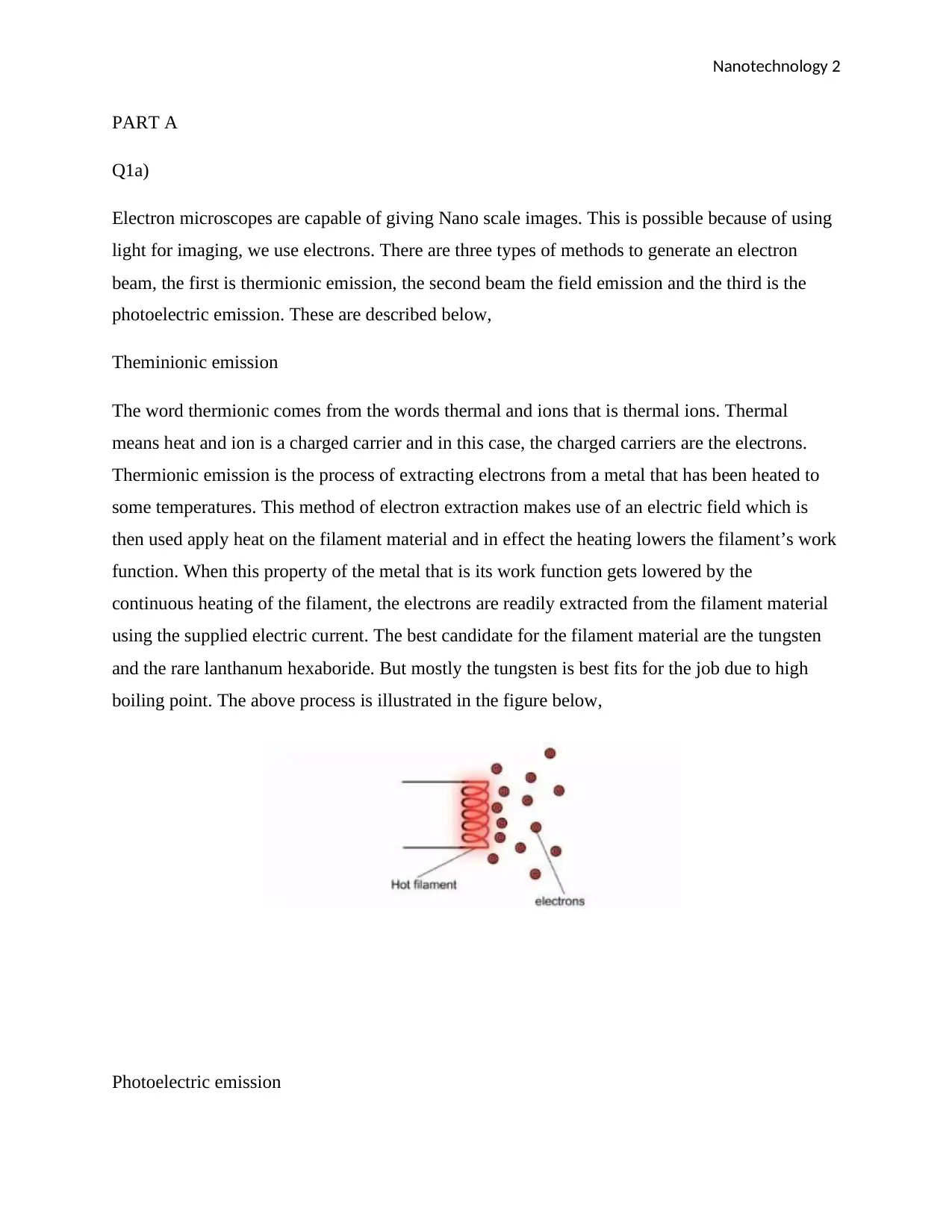
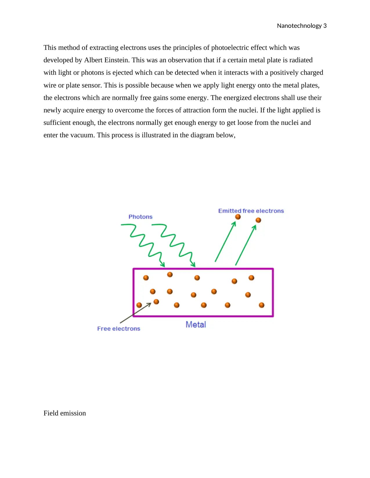
This nanotechnology assignment delves into the quantum mechanical principles underlying nanoscale phenomena and their practical applications. It explores various methods of electron emission, including thermionic, photoelectric, and field emission, detailing the processes and materials involved. The assignment addresses the Schrodinger equation and its implications for particle behavior at the nanoscale, including the concept of quantum tunneling. It further examines the density of states within energy bands and its relationship to material properties, alongside calculations involving Fermi energy and total energy. The solution discusses the limitations of Ohm's law at the nanoscale and explores the concept of quantum resistance. Finally, it investigates the phenomenon of Coulomb blockade in quantum dots, explaining its impact on conductance. This assignment provides a comprehensive overview of key concepts in nanotechnology, with detailed explanations and calculations, offering valuable insights into the behavior and applications of nanoscale materials and devices. Desklib provides a platform for students to access similar solved assignments and past papers.

Nanotechnology 1
NANOTECHNOLOGY
By Name
Course
Instructor
Institution
Location
Date
NANOTECHNOLOGY
By Name
Course
Instructor
Institution
Location
Date
Paraphrase This Document
Need a fresh take? Get an instant paraphrase of this document with our AI Paraphraser

Nanotechnology 2
PART A
Q1a)
Electron microscopes are capable of giving Nano scale images. This is possible because of using
light for imaging, we use electrons. There are three types of methods to generate an electron
beam, the first is thermionic emission, the second beam the field emission and the third is the
photoelectric emission. These are described below,
Theminionic emission
The word thermionic comes from the words thermal and ions that is thermal ions. Thermal
means heat and ion is a charged carrier and in this case, the charged carriers are the electrons.
Thermionic emission is the process of extracting electrons from a metal that has been heated to
some temperatures. This method of electron extraction makes use of an electric field which is
then used apply heat on the filament material and in effect the heating lowers the filament’s work
function. When this property of the metal that is its work function gets lowered by the
continuous heating of the filament, the electrons are readily extracted from the filament material
using the supplied electric current. The best candidate for the filament material are the tungsten
and the rare lanthanum hexaboride. But mostly the tungsten is best fits for the job due to high
boiling point. The above process is illustrated in the figure below,
Photoelectric emission

Nanotechnology 3
This method of extracting electrons uses the principles of photoelectric effect which was
developed by Albert Einstein. This was an observation that if a certain metal plate is radiated
with light or photons is ejected which can be detected when it interacts with a positively charged
wire or plate sensor. This is possible because when we apply light energy onto the metal plates,
the electrons which are normally free gains some energy. The energized electrons shall use their
newly acquire energy to overcome the forces of attraction form the nuclei. If the light applied is
sufficient enough, the electrons normally get enough energy to get loose from the nuclei and
enter the vacuum. This process is illustrated in the diagram below,
Field emission
⊘ This is a preview!⊘
Do you want full access?
Subscribe today to unlock all pages.

Trusted by 1+ million students worldwide

Nanotechnology 4
Field emission method of electron emission is a valid demonstration of the quantum mechanical
effects that occur is metal surfaces. This invention was made possible by Erwin Muller in the
1936. The device used for imaging images the crystalline structure of the tungsten needle tip.
The needle tip which usually of a radius of one micron, is in the center of a spherical glass bulb
under high vacuum. With over 10000 volts applied, the electric field is so strong at the needle tip
that electrons are spontaneously emitted to travel along the radial field line and impact on a zinc
sulfide screen of radius 5cm
Q1b
From the Schrodinger’s equations
-h2/2m * d2p(x)/dx2=(E-V) px
but
p(x)=Ae-(√2m(V-E/) h2*x
V represents the particle potential energy. To the left of the barrier, the particle does not
experience any potential energy because nothing is compelling it to move in a certain way so
V=0
The particle has only its energy moving it around E. h is the Planck’s constant. M is the mass.
The probability of finding the particle inside the barrier if the barrier potential energy is greater
than the particles energy that is V>E
Paraphrase This Document
Need a fresh take? Get an instant paraphrase of this document with our AI Paraphraser

Nanotechnology 5
p(x)=e(√2m(pos)/h2) *x
p(x)=e-x (positive #)
This represent the particle decay.
substituting back for β=(2π/h)2m[Uo-E]1/2
We get p(x)=e-2β
Q1c
(i)
The Richardson equation is used to find show the relationship between current density of a
thermionic emission to the work function(W) and the temperature of the material emitting the
electrons.
js=A T2 exp(-W/kT) …………………. (1)
js=current density of the emission given is (mA/mm2)
A=Richardson’s constant A=4*nmek2/h^3 which is approximately 1202mA/mm2K2 where m is the
mass and e is elementary charge and his plank’s constant
K is the Boltzman constant given by 8.6173324E-5 eV K-1
making the temperature the subject of the equation (1)
T==js/(A*exp(-W/K)

Nanotechnology 6
but js= 6.1*1010 Am-2
A=5*105 A m-2 K-2
K=8.6173324E-5
therefore, T=js= 6.1*1010 Am-2/ (5*105 *8.6173324E-5)
T=1415751352.471908824 K
Q1c
(ii)
𝐺 =2𝑒2
ℎ 𝑁
Where G=is the resistivity
N=number of channels
H=plank’s constant
e=energy of particles
making e subject of the formulae
𝑒2 = 𝐺ℎ
2𝑁
𝑒 =√ 𝐺ℎ
2𝑁
Substituting we get
⊘ This is a preview!⊘
Do you want full access?
Subscribe today to unlock all pages.

Trusted by 1+ million students worldwide

Nanotechnology 7
G=7.3995 ∗ 6.62607004 ×
10 −34
8
E=6.129*10-34 KJ
Wavelength
Wavelength= E*W/h
=6.129*10-34/6.62607004*10-34
=0.925nm
Q2a)
Atoms consist of nucleus with electrons orbiting around it and this orbits are in discrete shells.
For example, Lithium has 3 protons, 4 neutrons and 3 electrons when in neutral state. This makes
Lithium have one electrons loose in its outermost shell when we do an electronic configuration
of Lithium that is the Valence band. The one valence electron under different potential is free to
move. This particular shell is also called the conduction band in other words it does not require
energy to become conductor
Let’s represent the valence and conduction bands by two boxes. The conductor has a conduction
band that overlaps the valence bands as shown below. Because they overlap, every electron that
is in the valence band, is automatically in the conduction band, in other way, outermost electrons
are free to conduct.
There are millions of electrons and therefore millions of energy levels will be formed, and this
energy levels are very close to each other. This energy levels which are formed because of the
influence of the surrounding atoms in Lithium forms clusters. This clusters of energy levels
forms the bands
Paraphrase This Document
Need a fresh take? Get an instant paraphrase of this document with our AI Paraphraser

Nanotechnology 8
Q2b
Density of states
There are many energy levels in a particular band, that we know. Now we want to know how
many are their per unit energy that is what is the distribution of this states within the band and
that is what we mean by density of state
Density of state=No of states per unit energy per unit volume within that particular band
but separation between levels is inversely proportional to the interaction of atoms
Separation between levels ∝ 1/Interaction of atoms
Let g(E)=a function of density state
g(E)d(E) can be defined as the number of states g(E) in the energy interval E E+dE per
unit volume
When we Integrate
𝑆𝑣(𝐸′ ) = ∫ 𝑔 (𝐸)𝑑(𝐸)
𝐸′
0
Sv gives the total number of states below E’ per unit volume.
Consider electron in a 3D potential well.
We know for 3D potential well
𝐸 = ( ℎ2
8𝑚2𝐿2 )
L=Size of each side of the cube
N=integers
Because it is a solid, L is much larger than the latex parameter a

Nanotechnology 9
L>> a
Limiting our self to only free electrons in the state, we then we can arrive at the density.
Any particular combinations of n1. n2, n3
𝜑𝑛1, 𝑛2, 𝑛3
N12+n22+n32=(𝐸′ /ℎ^2) ∗ 8𝑚𝑒𝐿^2
Maximum value =n12
For a 3D space, we consider a sphere which will satisfy the equation n12+n22+n32=ni2
Here we look at the 1/8th of the sphere.
𝜑𝑛1𝑛2𝑛3 𝑒𝑎𝑐ℎ 𝑜𝑐𝑐𝑢𝑝𝑦 𝑎 𝑢𝑛𝑖𝑡 𝑣𝑜𝑙𝑢𝑚𝑒
Volume =1/8*4/3πni3
Sorb(ni)=πn3/6
Each orbit space can accommodate 2 electrons
Sn(ni)=2*πn3/3
But ni2=(𝐸′ /ℎ^2)8 m2L2
Substitute the value of S€=πL3/3h3(8meE’) ^3/2
Now what is L3??
This is the volume of the solid.
Now when we think in terms of unit volume
⊘ This is a preview!⊘
Do you want full access?
Subscribe today to unlock all pages.

Trusted by 1+ million students worldwide

Nanotechnology 10
Sv(E’)=π/3h3(8meE’)
Number of state per unit volume below E’ is got by differentiating with respect to g will give us
the density of state.
G€=𝑑𝑆𝑣(𝐸′ )
𝑑𝐸
(8𝜋21
2 ) (𝑚𝑒
ℎ2 )3 2⁄
(E’^1/2)
But the first two are just contants
Meaning essentially
G€ α E^1/2
G€ α (Etop – E)
Q2c
(i)
We know that for a 3D
𝑢 = 𝐴𝑒′(𝑞𝑥𝑋+𝑞𝑦+𝑌+𝑞𝑧)
But the density of state is given by
𝑔(𝑤) = 3 𝑉
2𝜋2 𝜔2
Making 𝜔the subject of the equation
𝜔 =√
𝑔(𝑤)2𝜋2
3𝑉
But
V=1.0*10-3
Π=3.142
Paraphrase This Document
Need a fresh take? Get an instant paraphrase of this document with our AI Paraphraser

Nanotechnology 11
g(w) =8920
therefore
ω=8920∗2∗3.1422
3∗10−3
=5.8706*107 electrons
(ii)
Fermi energy E is given by
𝐸 =ℎ2𝑘2
2𝑚
But m is the mass. m is given by the equation
𝑚 = 𝜌 ∗ 𝑣
But k is
𝑘 = 𝜋32
2
Therefore
𝐸 =
ℎ2 ∗ 𝜋32
2
2 ∗ 𝜌 ∗ 𝑉
6.62607004 ∗ 10−34 ∗ 3.14223
2
2 ∗ 8920 ∗ 10−3
5.6867 ∗ 10−30𝐽
iii)
Total energy g(E) is given by the formula
𝑔(𝐸) = 1
2𝜋2
2𝑀
ℎ2
3
2
𝐸
1
2

Nanotechnology 12
But M=𝜌 ∗ 𝑉
Therefore
𝑔(𝐸) = 1
2𝜋2
2 ∗ 𝜌 ∗ 𝑉
ℎ2
3
2
∗ 𝐸
1
2
Substituting the value for the parameter we get
𝑔(𝐸) = 1
23.1422
2 ∗ 8920 ∗(10)−3
(6.6260700 ∗ 10−34)2
3
2
∗(5.6867 ∗ 10−30)1
2
39.75 ∗ 1047𝐽
Q3a
I)
Although the ohm’s law is one of the basic law in electricity which relates the voltage, current
and resistance or impedance of a conductor, there are some limitation to the validity of this law.
First ohm’s law cannot be valid for unilateral networks like the diode which normally don’t have
the same current passing through them for the different current direction. This is contrary to the
ohms las which assumes the current is applied equally through the conduct.
Second, ohms law cannot be valid with the usage of non-linear elements with varying surface
area exposed to the electric current. Materials such as electric arc have their surface area change
hence difficult to estimate resistivity using the ohm’s law.
ii)
A wire with a single chain of electrons is expected to have a massive increase in the resistance
due to decrease in the surface area of the atoms exposed to the electric current. This decrease in
effect increases the resistance going by the ohm’s law. The atoms being closely packed will
again increase the resistivity since more current shall be flowing through them per unit areas.
This increase in current flow contributes to 5the massive resistivity of the single atom chain.
⊘ This is a preview!⊘
Do you want full access?
Subscribe today to unlock all pages.

Trusted by 1+ million students worldwide
1 out of 60

Your All-in-One AI-Powered Toolkit for Academic Success.
+13062052269
info@desklib.com
Available 24*7 on WhatsApp / Email
Unlock your academic potential
Copyright © 2020–2025 A2Z Services. All Rights Reserved. Developed and managed by ZUCOL.