Operational Amplifier Circuit Analysis and Design: DADC TMA1 Solution
VerifiedAdded on 2022/09/08
|10
|1200
|23
Homework Assignment
AI Summary
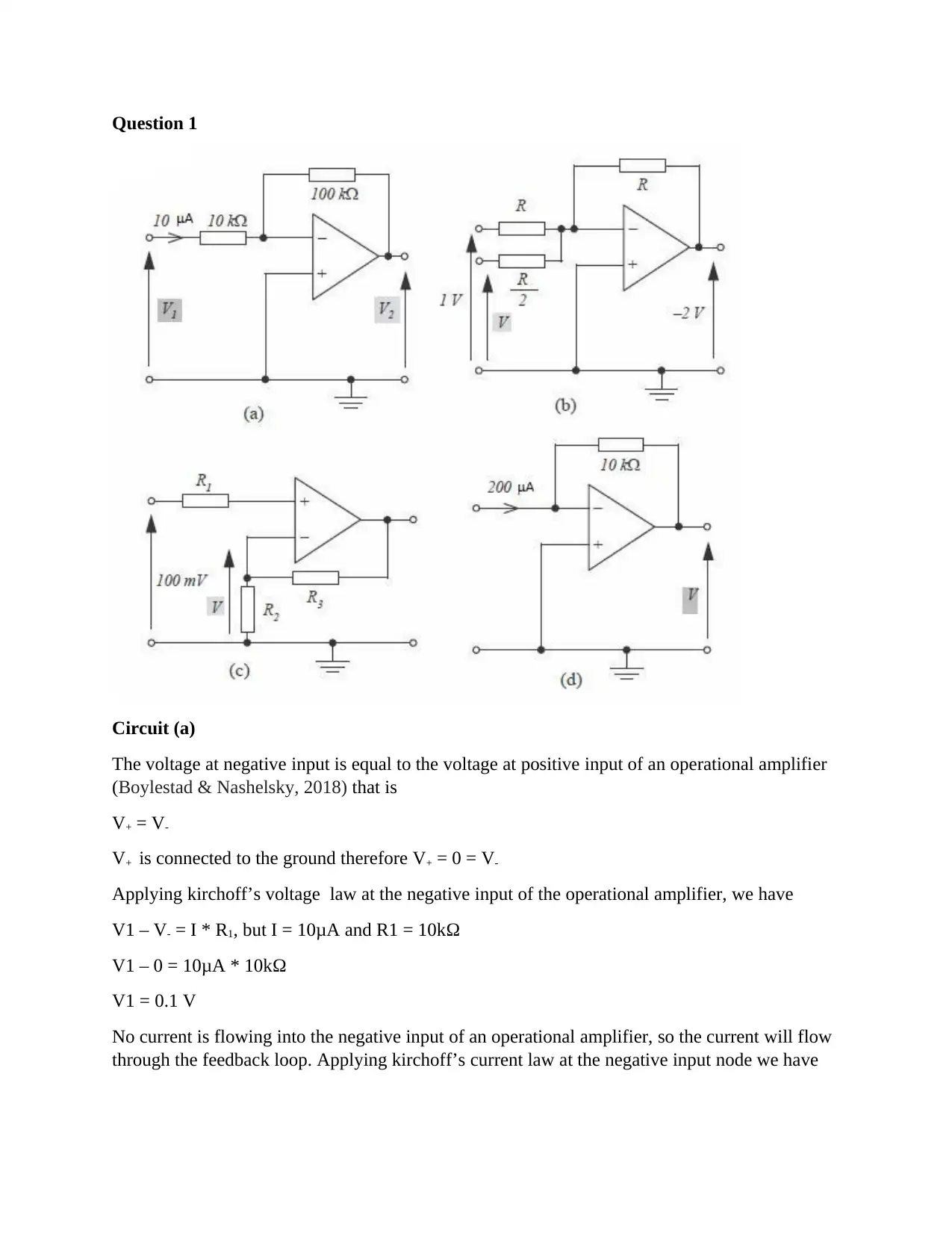
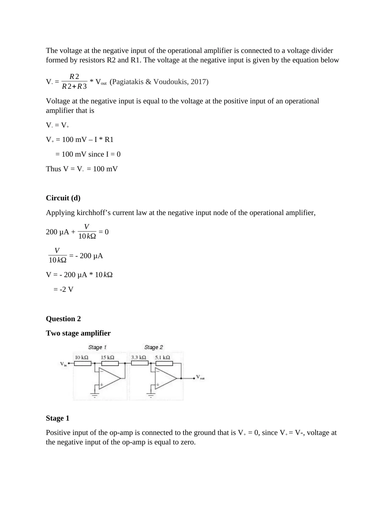
This document provides a comprehensive solution to a Digital & Analogue Devices & Circuits (DADC) TMA1 assignment, focusing on operational amplifiers (op-amps). The solution begins with the analysis of basic op-amp circuits, including inverting and non-inverting configurations, using Kirchhoff's laws and voltage divider principles. It then delves into the analysis of a two-stage amplifier, calculating the voltage gain of each stage and the overall gain. Finally, the solution examines an inverting operational amplifier comparator, analyzing its behavior and determining upper and lower threshold voltages, supported by simulation results. The document references relevant literature and provides a detailed explanation of each step, making it a valuable resource for students studying electronics and circuit analysis. The solution is designed to help students understand and solve problems related to operational amplifiers and their applications.

Question 1
Circuit (a)
The voltage at negative input is equal to the voltage at positive input of an operational amplifier
(Boylestad & Nashelsky, 2018) that is
V+ = V-
V+ is connected to the ground therefore V+ = 0 = V-
Applying kirchoff’s voltage law at the negative input of the operational amplifier, we have
V1 – V- = I * R1, but I = 10μA and R1 = 10kΩ
V1 – 0 = 10μA * 10kΩ
V1 = 0.1 V
No current is flowing into the negative input of an operational amplifier, so the current will flow
through the feedback loop. Applying kirchoff’s current law at the negative input node we have
Paraphrase This Document
Need a fresh take? Get an instant paraphrase of this document with our AI Paraphraser

10μA + V 2
100 kΩ = 0
10μA * 100 kΩ + V2 = 0
V2 = -1V
Circuit (b)
The voltage at the positive input of an operational amplifier is equal to zero since it is connected
to ground.And since voltage at the negative input is equal to the voltage at a positive input,
voltage at the negative input of an amplifier is equal to zero.
Applying Kirchhof’s current law at the negative input of operational amplifier we have
IR + IR/2 = IRf
1
R + V
R/2 = 2
R
1
R + 2∗V
R = 2
R . Multiplying both sides by R we get
1 + 2V = 2
Making V the subject we get
V = ½ V
Alternatively
The relationship between the input and output of a summing amplifier is given by the equation
below
Vout = - Rf
Rin Vin1 - Rf
R 2 n Vin2 (Neamen, 2001)
-2 = - R
R * 1 - R
R /2V
Making V the subject of the formula
V = ½ V
Circuit (c)
The circuit © is a non-inverting amplifier

The voltage at the negative input of the operational amplifier is connected to a voltage divider
formed by resistors R2 and R1. The voltage at the negative input is given by the equation below
V- = R 2
R 2+ R 3 * Vout (Pagiatakis & Voudoukis, 2017)
Voltage at the negative input is equal to the voltage at the positive input of an operational
amplifier that is
V- = V+
V+ = 100 mV – I * R1
= 100 mV since I = 0
Thus V = V- = 100 mV
Circuit (d)
Applying kirchhoff’s current law at the negative input node of the operational amplifier,
200 μA + V
10 kΩ = 0
V
10 kΩ = - 200 μA
V = - 200 μA * 10 kΩ
= -2 V
Question 2
Two stage amplifier
Stage 1
Positive input of the op-amp is connected to the ground that is V+ = 0, since V+ = V-, voltage at
the negative input of the op-amp is equal to zero.
⊘ This is a preview!⊘
Do you want full access?
Subscribe today to unlock all pages.

Trusted by 1+ million students worldwide

From kirchhof’s voltage law
Vin – V- = Iin * Rin
Vin = Iin * Rin since V- = 0
V- - Vout = If * Rf
Vout = - If * Rf
Voltage gain, Av = Vout / Vin
= - If * Rf / Iin * Rin
If = Iin since no current flows into the operational amplifier
Rf = 15kΩ
Rin = 10kΩ
Voltage gain, Av = Vout / Vin (Kumawat & Pathak, 2016)
= - If * Rf / Iin * Rin
= -15kΩ / 10kΩ
= - 1.5
Stage 2
From kirchhoff’s voltage law
Vin – V- = Iin * Rin
Vin = Iin * Rin since V- = 0
V- - Vout = If * Rf
Vout = - If * Rf
Voltage gain, Av = Vout / Vin
= - If * Rf / Iin * Rin
If = Iin since no current flows into the operational amplifier
Rf = 5.1 kΩ
Rin = 3.3 kΩ
Voltage gain, Av = Vout / Vin
= - If * Rf / Iin * Rin
= -5.1 kΩ / 3.3 kΩ
Vin – V- = Iin * Rin
Vin = Iin * Rin since V- = 0
V- - Vout = If * Rf
Vout = - If * Rf
Voltage gain, Av = Vout / Vin
= - If * Rf / Iin * Rin
If = Iin since no current flows into the operational amplifier
Rf = 15kΩ
Rin = 10kΩ
Voltage gain, Av = Vout / Vin (Kumawat & Pathak, 2016)
= - If * Rf / Iin * Rin
= -15kΩ / 10kΩ
= - 1.5
Stage 2
From kirchhoff’s voltage law
Vin – V- = Iin * Rin
Vin = Iin * Rin since V- = 0
V- - Vout = If * Rf
Vout = - If * Rf
Voltage gain, Av = Vout / Vin
= - If * Rf / Iin * Rin
If = Iin since no current flows into the operational amplifier
Rf = 5.1 kΩ
Rin = 3.3 kΩ
Voltage gain, Av = Vout / Vin
= - If * Rf / Iin * Rin
= -5.1 kΩ / 3.3 kΩ
Paraphrase This Document
Need a fresh take? Get an instant paraphrase of this document with our AI Paraphraser

= - 1.545
Overall gain
Av1 * AV2 = -1.5 * -1.545
= 2.3175
Question 3
a)
The figure above shows the input signal and the circuit of inverting operational amplifier
comparator. Comparator compares a input voltage with a reference voltage (V4 for the circuit b)
and produces a resultant signal at its output based on the comparison between the two voltages.
When the input voltage is less than reference voltage, the output of an operational amplifier
comparator swings towards its positive and input voltage is greater than the reference voltage
comparator output swings towards the negative rail (Link & Lee, 2018).
There is no flow of current into the positive input of the operational amplifier, therefore flow of
current from reference voltage V4 will flow through the voltage divider to the output of the
comparator.
At the voltage divider, voltage equation is given by the equation
V = Vref∗R 1
R 1+ R 2 + V 0∗R 2
R 1+ R 2

When the comparator’s output voltage is at its maximum positive swing, the threshold voltage is
given by
V+H = Vref∗R 1
R 1+ R 2 + V H∗R 2
R 1+ R 2 , (Nilsson & Riedel, 2015)
where VH = the maximum output swing = + 3 V and Vref = V4 = 3 V
= 3∗1000
1000+1000 + 3∗1000
1000+1000,
= 1.5 + 1.5
= 3. 0 V
Similarly when the comparator’s output voltage is at the lowest level, the threshold voltage is
given by
V+L = Vref∗R 1
R 1+ R 2 + V L∗R 2
R 1+ R 2 , where VL = the lowest output swing = - 3 V and Vref = V4 = 3 V
= 3∗1000
1000+1000 + −3∗1000
1000+1000,
= 1.5 - 1.5
= 0 V
b)
given by
V+H = Vref∗R 1
R 1+ R 2 + V H∗R 2
R 1+ R 2 , (Nilsson & Riedel, 2015)
where VH = the maximum output swing = + 3 V and Vref = V4 = 3 V
= 3∗1000
1000+1000 + 3∗1000
1000+1000,
= 1.5 + 1.5
= 3. 0 V
Similarly when the comparator’s output voltage is at the lowest level, the threshold voltage is
given by
V+L = Vref∗R 1
R 1+ R 2 + V L∗R 2
R 1+ R 2 , where VL = the lowest output swing = - 3 V and Vref = V4 = 3 V
= 3∗1000
1000+1000 + −3∗1000
1000+1000,
= 1.5 - 1.5
= 0 V
b)
⊘ This is a preview!⊘
Do you want full access?
Subscribe today to unlock all pages.

Trusted by 1+ million students worldwide

c) Screen shot of circuit used in simulation
Paraphrase This Document
Need a fresh take? Get an instant paraphrase of this document with our AI Paraphraser

Input and output waveforms of inverting operational amplifier comparator
Upper and lower thresholds voltage from simulated results are 2.5 V and 0 V respectively
whereas the upper and lower threshold voltages from calculated results are 3 V and 0 V
Upper and lower thresholds voltage from simulated results are 2.5 V and 0 V respectively
whereas the upper and lower threshold voltages from calculated results are 3 V and 0 V

respectively. The slight variation in upper threshold voltage is due to inverter comparator’s offset
voltage (Perner, Eldredge & Tran, 2011).
REFERENCE LIST
voltage (Perner, Eldredge & Tran, 2011).
REFERENCE LIST
⊘ This is a preview!⊘
Do you want full access?
Subscribe today to unlock all pages.

Trusted by 1+ million students worldwide

Boylestad, R. L., & Nashelsky, L. (2018). Electronic Devices and Circuit Theory 11th ed.
Kumawat, J., & Pathak, P. (2016). Analysis of Operational Amplifier using 120 nm Technology.
Link, G. N., & Lee, W. (2018). U.S. Patent Application No. 15/983,610.
Neamen, D. A. (2001). Electronic circuit analysis and design (Vol. 2). New York, NY.:
McGraw-Hill.
Nilsson, J. W., & Riedel, S. A. (2015). Electric circuits. Upper Saddle River, NJ: Pearson.
Pagiatakis, G., & Voudoukis, N. (2017). Operational amplifiers teaching and students'
understanding. In 2017 IEEE Global Engineering Education Conference (EDUCON) (pp.
312-316). IEEE.
Perner, F. A., Eldredge, K. J., & Tran, L. T. (2011). U.S. Patent No. 6,262,625. Washington, DC:
U.S. Patent and Trademark Office.
1 out of 10

Your All-in-One AI-Powered Toolkit for Academic Success.
+13062052269
info@desklib.com
Available 24*7 on WhatsApp / Email
Unlock your academic potential
Copyright © 2020–2025 A2Z Services. All Rights Reserved. Developed and managed by ZUCOL.