University Filter Design and Analysis: ENG530 Portfolio, 2018/2019

Verified

Added on  2022/08/27

|22
|2204
|17
Practical Assignment
AI Summary
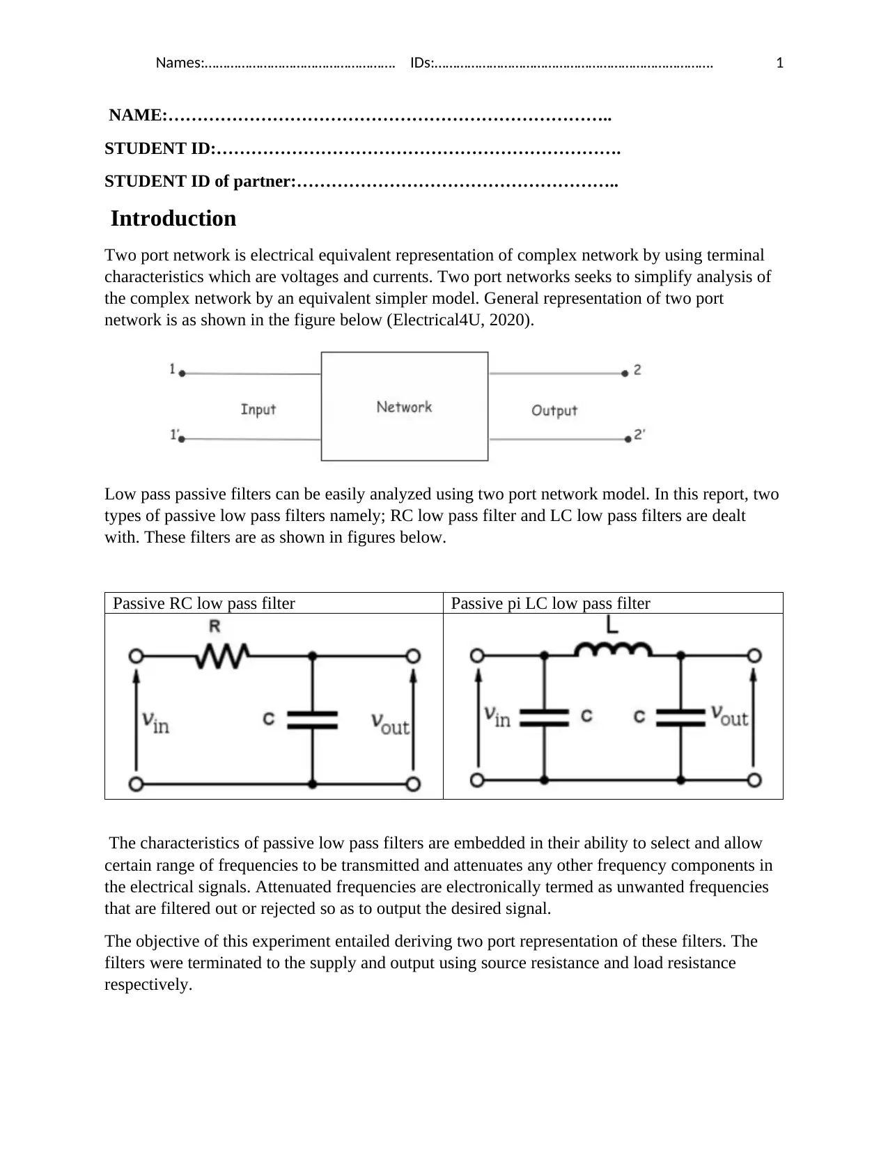
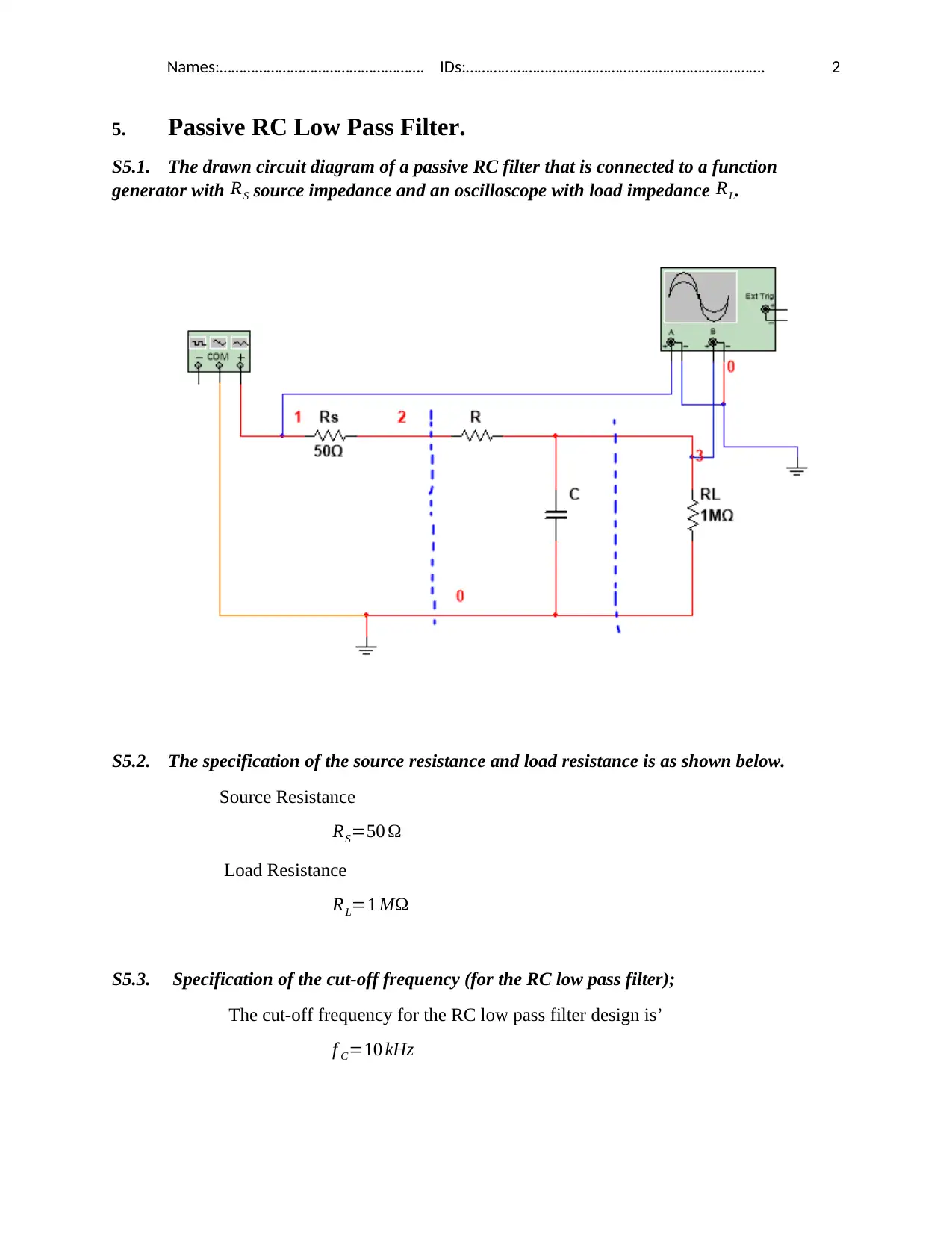
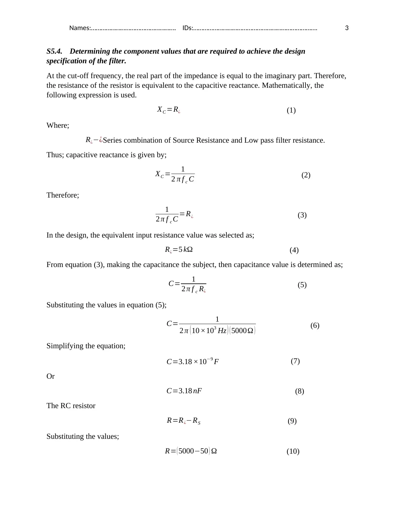
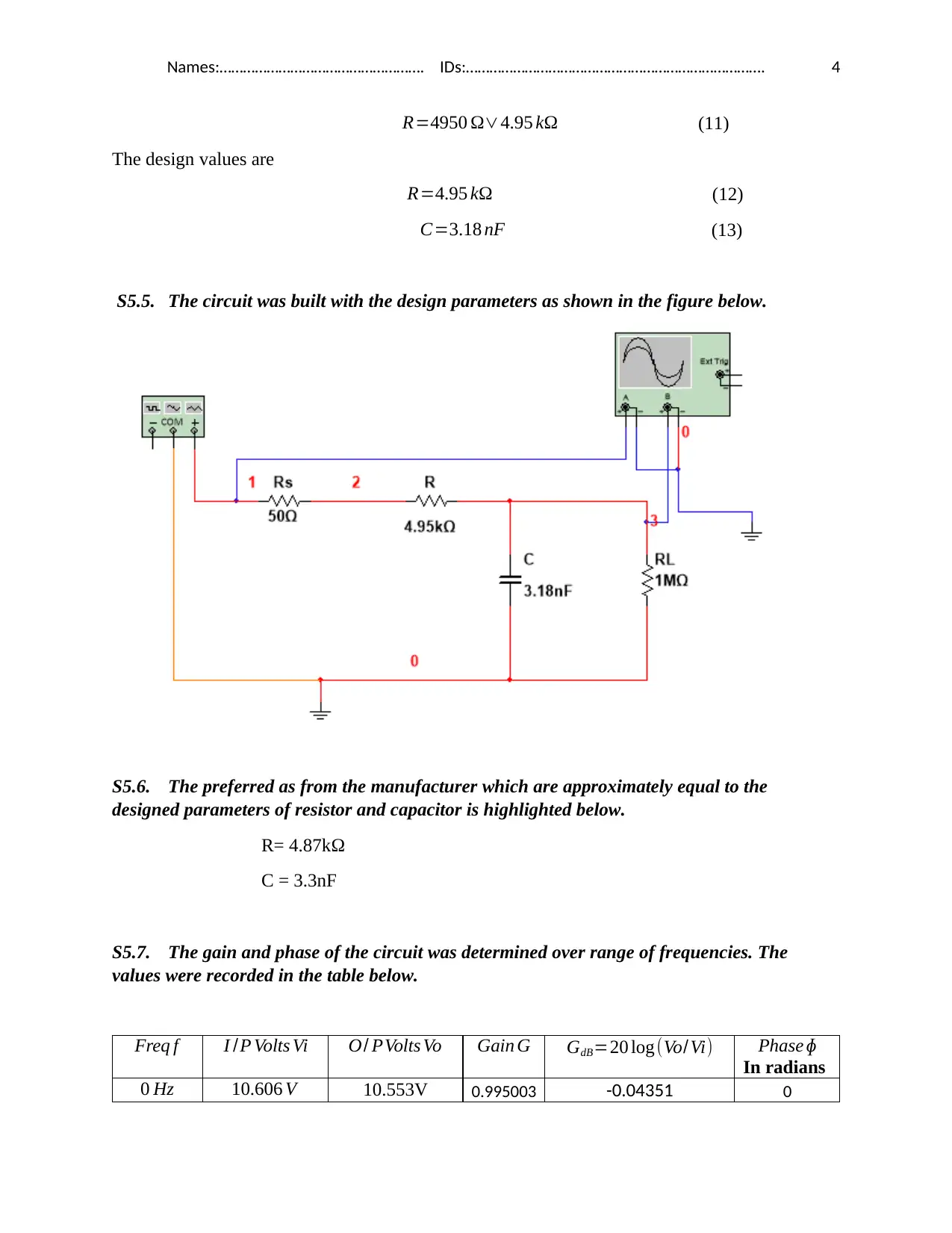
This report presents a practical assignment focused on the design, analysis, and implementation of passive low-pass filters, specifically RC and LC types, within the context of the ENG530 Analogue Analysis and Design course. The assignment utilizes the two-port network representation to simplify the analysis of complex electrical circuits. The student details the design process for both filter types, including the determination of component values based on specified cut-off frequencies and source/load resistances. The report includes circuit diagrams, component specifications, experimental measurements of gain and phase responses across varying frequencies, and graphical representations of the magnitude and phase responses. Transfer functions for both filters are derived, and two-port representations are established using impedance parameters. The report concludes with a comparison of theoretical and experimental results, highlighting sources of error and discussing the filters' characteristics and performance. The assignment demonstrates the student's ability to apply theoretical knowledge to practical circuit design and analysis, a core objective of the course.
Document Page
Names:……………………………………………. IDs:…………………………………………………………………. 1
NAME:…………………………………………………………………..
STUDENT ID:…………………………………………………………….
STUDENT ID of partner:………………………………………………..
Introduction
Two port network is electrical equivalent representation of complex network by using terminal
characteristics which are voltages and currents. Two port networks seeks to simplify analysis of
the complex network by an equivalent simpler model. General representation of two port
network is as shown in the figure below (Electrical4U, 2020).
Low pass passive filters can be easily analyzed using two port network model. In this report, two
types of passive low pass filters namely; RC low pass filter and LC low pass filters are dealt
with. These filters are as shown in figures below.
Passive RC low pass filter Passive pi LC low pass filter
The characteristics of passive low pass filters are embedded in their ability to select and allow
certain range of frequencies to be transmitted and attenuates any other frequency components in
the electrical signals. Attenuated frequencies are electronically termed as unwanted frequencies
that are filtered out or rejected so as to output the desired signal.
The objective of this experiment entailed deriving two port representation of these filters. The
filters were terminated to the supply and output using source resistance and load resistance
respectively.
tabler-icon-diamond-filled.svg

Paraphrase This Document

Need a fresh take? Get an instant paraphrase of this document with our AI Paraphraser
Document Page
Names:……………………………………………. IDs:…………………………………………………………………. 2
5. Passive RC Low Pass Filter.
S5.1. The drawn circuit diagram of a passive RC filter that is connected to a function
generator with RS source impedance and an oscilloscope with load impedance RL.
S5.2. The specification of the source resistance and load resistance is as shown below.
Source Resistance
RS=50 Ω
Load Resistance
RL=1
S5.3. Specification of the cut-off frequency (for the RC low pass filter);
The cut-off frequency for the RC low pass filter design is’
f C=10 kHz
Document Page
Names:……………………………………………. IDs:…………………………………………………………………. 3
S5.4. Determining the component values that are required to achieve the design
specification of the filter.
At the cut-off frequency, the real part of the impedance is equal to the imaginary part. Therefore,
the resistance of the resistor is equivalent to the capacitive reactance. Mathematically, the
following expression is used.
XC =R¿ (1)
Where;
R¿¿Series combination of Source Resistance and Low pass filter resistance.
Thus; capacitive reactance is given by;
XC = 1
2 π f c C (2)
Therefore;
1
2 π f c C =R¿ (3)
In the design, the equivalent input resistance value was selected as;
R¿=5 (4)
From equation (3), making the capacitance the subject, then capacitance value is determined as;
C= 1
2 π f c R¿
(5)
Substituting the values in equation (5);
C= 1
2 π ( 10 ×103 Hz ) ( 5000Ω ) (6)
Simplifying the equation;
C=3.18 ×10⁹ F (7)
Or
C=3.18 nF (8)
The RC resistor
R=R¿RS (9)
Substituting the values;
R= ( 500050 ) Ω (10)
Document Page
Names:……………………………………………. IDs:…………………………………………………………………. 4
R=4950 Ω4.95 (11)
The design values are
R=4.95 (12)
C=3.18 nF (13)
S5.5. The circuit was built with the design parameters as shown in the figure below.
S5.6. The preferred as from the manufacturer which are approximately equal to the
designed parameters of resistor and capacitor is highlighted below.
R= 4.87kΩ
C = 3.3nF
S5.7. The gain and phase of the circuit was determined over range of frequencies. The
values were recorded in the table below.
Freq f I /P Volts Vi O/ PVolts Vo Gain G GdB=20 log(Vo/Vi) Phase ɸ
In radians
0 Hz 10.606 V 10.553V 0.995003 -0.04351 0
tabler-icon-diamond-filled.svg

Paraphrase This Document

Need a fresh take? Get an instant paraphrase of this document with our AI Paraphraser
Document Page
Names:……………………………………………. IDs:…………………………………………………………………. 5
10 Hz 10.606 V 10.554V 0.995003 -0.04351 -0.001
100 Hz 10.606 V 10.553V 0.995003 -0.04351 -0.00999
1 kHz 10.606 V 10.502V 0.995003 -0.04351 -0.09961
10 kHz 10.606 V 7.473V 0.704601 -3.04113 -0.78519
100 kHz 10.606 V 1.053V 0.099283 -20.0625 -1.47156
1 MHz 10.606 V 0.1V 0.009429 -40.511 -1.56148
10 MHz 10.606 V 0.01V 0.000943 -60.511 -1.57038
S5.8. The magnitude response of the designed circuit was plotted on the logarithmic graph
as shown in the figure below.
Document Page
Names:……………………………………………. IDs:…………………………………………………………………. 6
S5.9. The phase response of the designed circuit was plotted in the logarithmic graph as
shown in the figure below.
S5.10. Graph measurements are shown below
(S5.10.1) The cut-off frequency is;
f c
Actual=12 kHz
(S5.10.2) The per decade slope of the gain magnitude is;
SActual
Decade=20 dB/decade
(S5.10.3) The per octave slope of the gain magnitude is;
SActual
Octave =6 dB
(S5.10.4) The passband phase in radians is;
θActual
Pass =0 ¿0.78519 radians
(S5.10.5)The stopband phase in radians is;
θActual
Stop =0.78519 radians
(S5.10.6)The phase radians at the cut-off frequency is
θActual
Cut off =0.78519 radians
Document Page
Names:……………………………………………. IDs:…………………………………………………………………. 7
(S5.10.7) Fractional percentage error between the cut-off frequency value and the one
specified in the design was computed as illustrated below.
Ef = f c
f design
×100 % (14)
Substituting the values;
Ef =(1210)kHz
10 kHz ×100 %=+20 % (15)
(S5.11) The circuit below was used to determine the transfer function of the passive RC low
pass filter.
The output voltage across Load resistance Rout of the circuit is equivalent to the voltage across the
capacitor.
V out = { ZC
Z R +ZC }V ¿ (16)
The transfer function is;
V out
V ¿
= ZC
ZR + ZC
(17)
The impedances of the circuit in the Laplace transform are as shown below.
ZC = 1
Cs (18)
And
ZR=Rin (19)
tabler-icon-diamond-filled.svg

Paraphrase This Document

Need a fresh take? Get an instant paraphrase of this document with our AI Paraphraser
Document Page
Names:……………………………………………. IDs:…………………………………………………………………. 8
The transfer function is therefore;
V out
V ¿
=H=
1
Cs
R+ 1
Cs
(20)
Algebraically rearranging the equation above
H= 1
RCs+1 (21)
Alternatively; by rewriting;
s=
Then the transfer function becomes;
H ( ) = 1
1+ jωRC (23)
Therefore, RC low pass filter is basically a first-order type filter
(S5.12) Deriving a two port representation for this circuit
Two port circuit of the network is generally represented by;
Basing on the Z-impedance model, general equations of two port network are as shown below.
V 1=Z11 I1 + Z12 I 2 (24)
V 2=Z21 I 1+Z22 I 2 (25)
Passive RC low pass filter is represented as shown below.
Document Page
Names:……………………………………………. IDs:…………………………………………………………………. 9
The model parameters are determined by individually setting currents to zero.
Assuming I 2=0.
Z11= V 1
I 1
=R¿ j
ωC (26)
Substituting the values;
Z11= (5000 j
2 π ( 5000 Hz ×3.18 ×109 F ) )Ω (27)
Simplifying equation (27)
Z11= ( 5000 j 10010 ) Ω (28)
Z11= (5 j 10 ) (29)
Also, when I2=0
Z21= V 2
I1
= j
2 πfC (30)
Substituting the values in the equation above;
Z21= j
2 π ( 5000 Hz ×3.18 ×109 F ) (31)
Simplifying the equation;
Z21= ( j 10010 ) Ω (32)
Z21= j 10
Document Page
Names:……………………………………………. IDs:…………………………………………………………………. 10
Assuming I 1=0.
Z12= V 1
I 2
= j
2 πfC (33)
Z12= j10 (34)
Also
Z22= V 2
I 2
= j
2 πfC (35)
Z22= j 10 (36)
6 Passive LC low pass filter
S6.1. The circuit diagram of a passive pi-type LC filter is as shown in the figure below. The
filter is connected to the function generator via the source resistance RS and as well as
connected to the oscilloscope via load resistance RL .
S6.2 The design specification of the cut-off frequency for the LC passive low pass filter is
provided in this section.
tabler-icon-diamond-filled.svg

Paraphrase This Document

Need a fresh take? Get an instant paraphrase of this document with our AI Paraphraser
Document Page
Names:……………………………………………. IDs:…………………………………………………………………. 11
The cut-off frequency of this pi type LC passive low pass filter was chosen as;
f c=15 kHz
S6.3 Determination of the right values of components that are required to achieve the
desired specifications.
The combination of capacitive reactance of C1C2 gives shunt equivalent impedance as;
Z2 =Zc1+ Zc2 (37)
Where;
Zc1=Zc2=1
2 Zc (38)
The product of shunt and series impedance gives a constant Rk . For instance, therefore;
Z1 Z2= ( Rk )2. (39)
Where;
Z1 = jωL and (40)
Z2 = j
ωC
Substituting equation (40) into equation (39);
( jωL ) ( j
ωC ) = ( Rk ) 2 (41)
Simplifying equation (41) algebraically;
L
C = ( Rk )2 (42)
Therefore, source impedance is expressed as;
Rk = L
C (43)
The characteristic impedance of the circuit is given by;
ZOT = z1
2
4 +Z1 Z2 (44)
Substituting the equivalent expressions;
Document Page
Names:……………………………………………. IDs:…………………………………………………………………. 12
ZOT = ( jωL ) 2
4 + L
C (45)
Algebraically simplifying the expression;
ZOT = L
C ( ωL )2
4 (46a)
ZOT = L
C 1 ω2 CL
4 (46b)
At cut-off frequency;
1 ω2 CL
4 =0 (47)
From equation (47), the cut-off frequency is given by;
ω2 CL
4 =1 (49a)
ω= 4
LC (49b)
Since;
ω=2 πf (50)
Then by substitution; the cut-off frequency in Hertz is given by;
f c= 1
π LC (51)
According to the design;
f c=15 kHz
And therefore with an inductance of 3mH
L=3 mH
Then from equation (51), the capacitance is given by;
C= 1
( π f c )2 L (52)
Substituting the values;
C= 1
( π ×15000 Hz )2 × ( 0.003 H ) (53a)
chevron_up_icon
1 out of 22
circle_padding
hide_on_mobile
zoom_out_icon
[object Object]