Comparative Study on Multichannel and U-Shaped Assembly Layout of PCB
VerifiedAdded on 2023/01/12
|12
|1807
|30
Report
AI Summary
This report presents a comparative study on multichannel and U-shaped assembly layouts for PCB assembly, utilizing Flexism simulation for educational purposes. The literature review introduces the importance of PCBs in modern electronics and the need for efficient assembly processes. It explores simulation as a tool for improving PCB assembly design, focusing on Surface Mount Technology (SMT) and Insertion Mount Technology (IMT) processes. The report details the steps involved in Flexism simulation, including data collection, model development, and output analysis. It emphasizes the use of simulation for educational purposes, highlighting how it creates a controlled learning environment and facilitates problem-solving in engineering. The report also touches upon performing cost and time analysis for assembly lines. The significance of simulation in PCB assembly lines and the importance of finding efficiency in assembly line layout is discussed. Finally, the report concludes with references to relevant literature.

Dissertation
Paraphrase This Document
Need a fresh take? Get an instant paraphrase of this document with our AI Paraphraser
Table of Contents
Topic: Comparative Study on Multichannel and U-Shaped Assembly Layout of PCB Assembly
using Flexism Simulation for Educational Purpose.........................................................................1
Literature Review.............................................................................................................................1
Steps for simulation.....................................................................................................................1
Simulation for educational purposes...........................................................................................1
Performing cost analysis for assembly lines................................................................................1
Performing time analysis for assembly lines...............................................................................1
Significance in simulation of PCB assembly lines......................................................................1
Significance of finding efficiency of assemble line layout.........................................................1
REFERENCES................................................................................................................................2

⊘ This is a preview!⊘
Do you want full access?
Subscribe today to unlock all pages.
Trusted by 1+ million students worldwide
Topic: Comparative Study on Multichannel and U-Shaped Assembly Layout
of PCB Assembly using Flexism Simulation for Educational Purpose
Literature Review
Introduction
Printed circuit boards or PCBs are unsung heroes present in modern electronic devices,
which is designed to help new as well as seasoned engineers, to make better informed decisions
in less period, to end up with appropriate and perfect components for product development. As
fundamental characteristic of competitive environment in today’s world includes the requirement
of shorter product life cycles as well as increased demands for the customization (Jo and Kim,
2018). But as these aspects seems to be difficult for satisfying operating via traditional
production lines. Therefore, JIT U-lines development is being the emerging response for
competing in such competing environment. The present literature review describes the
simulation utilization to guide the efforts for improvement while redesigning the PCB assembly.
A comparative study is done on U-shaped and multichannel layout of this assembly, by using
flexism simulation in educational purpose. The study is done to understand the PCB assembly
process by using simulation with flexism approach. To improve the overall performance of
system, feasibility of flow logic process is assessed, including impact of changing line
configuration.
Steps for simulation
Simulation of the electronic circuit mostly uses a number of mathematical models for
getting the actual behaviour of electronic devices like PCB (Printed circuit board). Simulation
software helps in modelling the electronic circuit operation. Through research, it has been
evaluated that before manufacturing, simulating the circuit behaviour helps in improving and
increasing the design efficiency. PCB designing which requires modelling like IBIS models,
transmission lines etc. so, simulator includes schematic editor, waveform display, simulation
engine and more, that monitors the effect also which may occur during operation. PCB or printed
circuit board assembly lines are mainly fall within serial production line general category. But
common problem that might be faced by engineers during designing configuration of future or
existing lines for meeting targeted production rates. Therefore, simulation modelling helps in
capturing the complex behaviour as well as interaction among various components of assembly
1
Paraphrase This Document
Need a fresh take? Get an instant paraphrase of this document with our AI Paraphraser
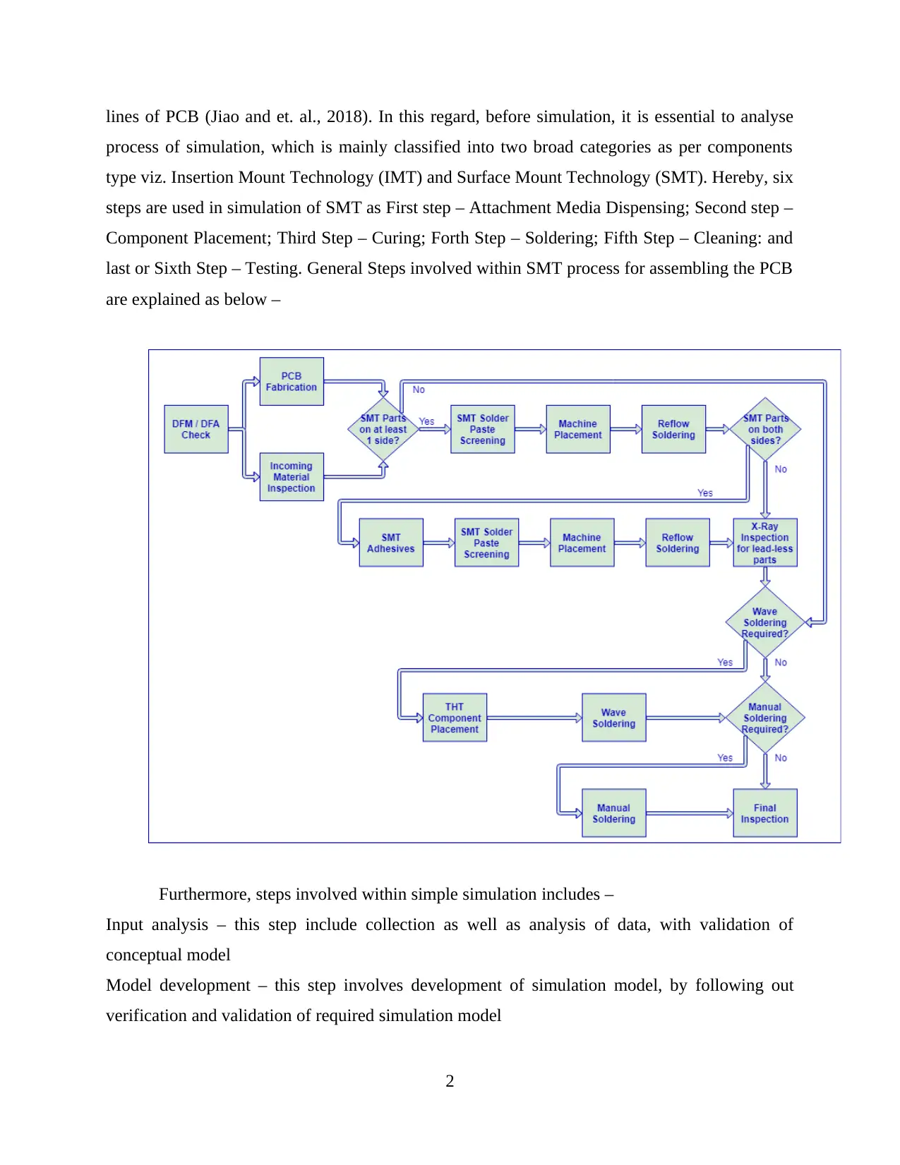
lines of PCB (Jiao and et. al., 2018). In this regard, before simulation, it is essential to analyse
process of simulation, which is mainly classified into two broad categories as per components
type viz. Insertion Mount Technology (IMT) and Surface Mount Technology (SMT). Hereby, six
steps are used in simulation of SMT as First step – Attachment Media Dispensing; Second step –
Component Placement; Third Step – Curing; Forth Step – Soldering; Fifth Step – Cleaning: and
last or Sixth Step – Testing. General Steps involved within SMT process for assembling the PCB
are explained as below –
Furthermore, steps involved within simple simulation includes –
Input analysis – this step include collection as well as analysis of data, with validation of
conceptual model
Model development – this step involves development of simulation model, by following out
verification and validation of required simulation model
2
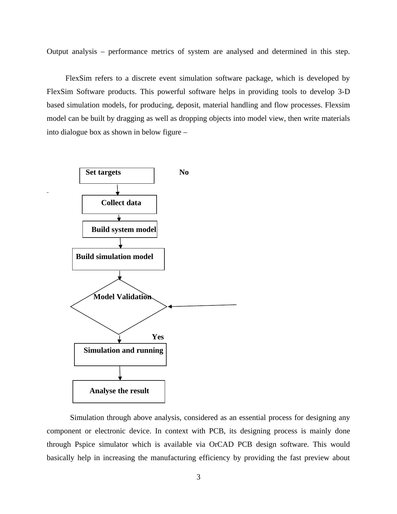
Output analysis – performance metrics of system are analysed and determined in this step.
FlexSim refers to a discrete event simulation software package, which is developed by
FlexSim Software products. This powerful software helps in providing tools to develop 3-D
based simulation models, for producing, deposit, material handling and flow processes. Flexsim
model can be built by dragging as well as dropping objects into model view, then write materials
into dialogue box as shown in below figure –
Set targets No
Collect data
Build system model
Build simulation model
Model Validation
Yes
Simulation and running
Analyse the result
Simulation through above analysis, considered as an essential process for designing any
component or electronic device. In context with PCB, its designing process is mainly done
through Pspice simulator which is available via OrCAD PCB design software. This would
basically help in increasing the manufacturing efficiency by providing the fast preview about
3
⊘ This is a preview!⊘
Do you want full access?
Subscribe today to unlock all pages.
Trusted by 1+ million students worldwide
how PCB after designing is going to look, as well as estimating its performance in different
application. If PCB involves any type of functional property such as speed, signals, frequency,
lower current and so on, then it is essential to integrate the best schematic layout for integrating
the system with specific simulation tools. Therefore, by simulating the PCB, parameters like
signal integrity, power delivery, mixed signal simulation and others, can easily be analysed.
Thus, for creating simulation in PCB assembly, it is required to create the simulation profile first,
under which process like selection of analysis type can be done, that can be refused also when
required. Hereby, through creation of simulation profile, editing and modifications also can be
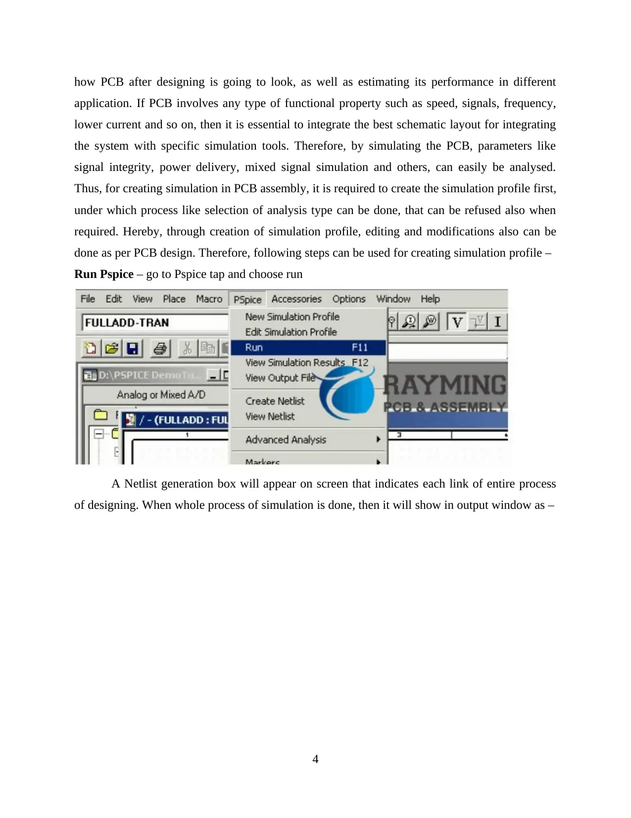
done as per PCB design. Therefore, following steps can be used for creating simulation profile –
Run Pspice – go to Pspice tap and choose run
A Netlist generation box will appear on screen that indicates each link of entire process
of designing. When whole process of simulation is done, then it will show in output window as –
4
application. If PCB involves any type of functional property such as speed, signals, frequency,
lower current and so on, then it is essential to integrate the best schematic layout for integrating
the system with specific simulation tools. Therefore, by simulating the PCB, parameters like
signal integrity, power delivery, mixed signal simulation and others, can easily be analysed.
Thus, for creating simulation in PCB assembly, it is required to create the simulation profile first,
under which process like selection of analysis type can be done, that can be refused also when
required. Hereby, through creation of simulation profile, editing and modifications also can be
done as per PCB design. Therefore, following steps can be used for creating simulation profile –
Run Pspice – go to Pspice tap and choose run
A Netlist generation box will appear on screen that indicates each link of entire process
of designing. When whole process of simulation is done, then it will show in output window as –
4
Paraphrase This Document
Need a fresh take? Get an instant paraphrase of this document with our AI Paraphraser
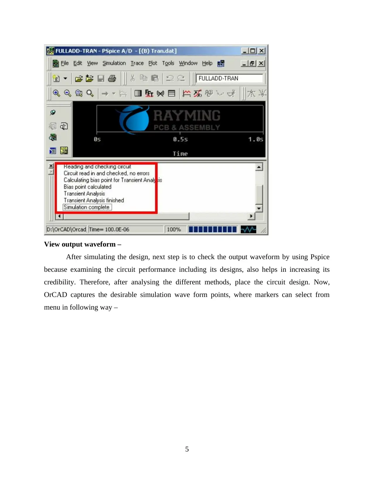
View output waveform –
After simulating the design, next step is to check the output waveform by using Pspice
because examining the circuit performance including its designs, also helps in increasing its
credibility. Therefore, after analysing the different methods, place the circuit design. Now,
OrCAD captures the desirable simulation wave form points, where markers can select from
menu in following way –
5
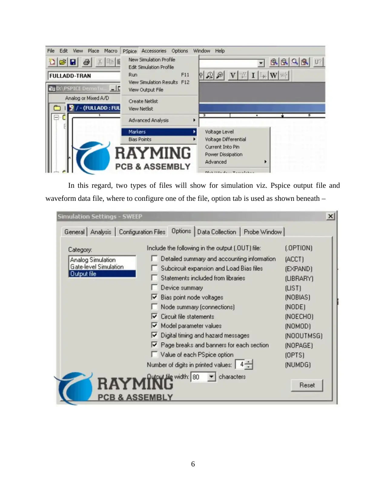
In this regard, two types of files will show for simulation viz. Pspice output file and
waveform data file, where to configure one of the file, option tab is used as shown beneath –
6
waveform data file, where to configure one of the file, option tab is used as shown beneath –
6
⊘ This is a preview!⊘
Do you want full access?
Subscribe today to unlock all pages.
Trusted by 1+ million students worldwide
Simulation for educational purpose
Simulations has created the real world process into controlled environment, therefore, in
educational field, it can be used for providing a creative learning environment for learners.
Simulation can be used in various ways, especially for scientific discovery, testing designs for
safety, creating graphics for providing education and more. For providing education in real life
or more visualise manner, a number of activities can be created that helps in promoting effective
learning. Having ambiguous and open-ended features, simulated learning activities encourage
learners for contemplating the scenario implications, by understanding the situation in real
manner and through experimental practices. In the field of engineering, Modelling and
simulation refers to a problem-solving methodology that helps learners in analysing the most
complex systems more easily. … defines the simulation in engineering as “The process
modelling that mimics response of the real or actual system to events which take place with
time”. While through perception of …, simulation is identified as process of designing a real
system model, that helps in conducting a number of experiments for understanding the system
behaviour, through which various strategies can be developed for operating the same and resolve
complex problems. Such model of real system can also be used for analysing the current
operations as well as identifying problem area such bottlenecks, testing different scenarios for
making improvement, designing new manufacturing systems for product development and more.
Simulation models allow learners to test the potential changes within existing system or
evaluating the new design system instead of building it.
Similarly, in the field of manufacturing sector, a number of simulation applications can be
used such as printed circuit board assembly (PCB), wafer fab production, surface mount
technological lines and in other assembly operations. As electronics is considered as the integral
part of daily lives, like smart phones to cars, so, all these things are possible only through PCB. It
is mainly found as small green chips which are covered in lines, made with fiber-glasses, copper
and various metals. PCB or Printed circuit board designs helps in bringing electronic circuits to
life, within physical form. By simulation, this design process combines a number of component
placements and routines, in order to define the electrical connectivity on manufactured board of
circuit. In PCB assembly, it involves total automated assembly lines, manual and semi-manual
etc., where these operations are integrated totally with test operations.
7
Paraphrase This Document
Need a fresh take? Get an instant paraphrase of this document with our AI Paraphraser
Performing cost analysis for assembly lines
Performing time analysis for assembly lines
Significance in simulation of PCB assembly lines
Significance of finding efficiency of assemble line layout
Conclusion
8
Performing time analysis for assembly lines
Significance in simulation of PCB assembly lines
Significance of finding efficiency of assemble line layout
Conclusion
8
REFERENCES
Books and Journals
Jiao, Y. L. and et. al., 2018. Multi-objective storage location allocation optimization and
simulation analysis of automated warehouse based on multi-population genetic
algorithm. Concurrent Engineering. 26(4). pp.367-377.
Jo, D. S. and Kim, J. W., 2018. A survey on characteristics and application domains of 3D
factory simulation technology. The Journal of Information Systems. 27(4). pp.35-70.
Trung, N. K. and et. al., 2015. Analysis and PCB design of class D inverter for wireless power
transfer systems operating at 13.56 MHz. IEEJ Journal of Industry Applications. 4(6).
pp.703-713.
Bohnhorst, A., Kirk, A. T. and Zimmermann, S., 2016. Simulation aided design of a low cost ion
mobility spectrometer based on printed circuit boards. International Journal for Ion
Mobility Spectrometry. 19(2-3). pp.167-174.
Fitzpatrick, D., 2017. Analog design and simulation using OrCAD Capture and PSpice. Newnes.
Ajao, L. A. and et. al., 2016. Learning of embedded system design, simulation and
implementation: A technical approach. American Journal of Embedded Systems and
Applications. 3(3). pp.35-42.
9
⊘ This is a preview!⊘
Do you want full access?
Subscribe today to unlock all pages.
Trusted by 1+ million students worldwide
1 out of 12


Your All-in-One AI-Powered Toolkit for Academic Success.
+13062052269
info@desklib.com
Available 24*7 on WhatsApp / Email
![[object Object]](/_next/static/media/star-bottom.7253800d.svg)
Unlock your academic potential
Copyright © 2020–2026 A2Z Services. All Rights Reserved. Developed and managed by ZUCOL.