Analysis of Photovoltaic Cell Technology: Research on Energy Solutions

Verified

Added on  2023/06/07

|7
|1708
|68
Report
AI Summary
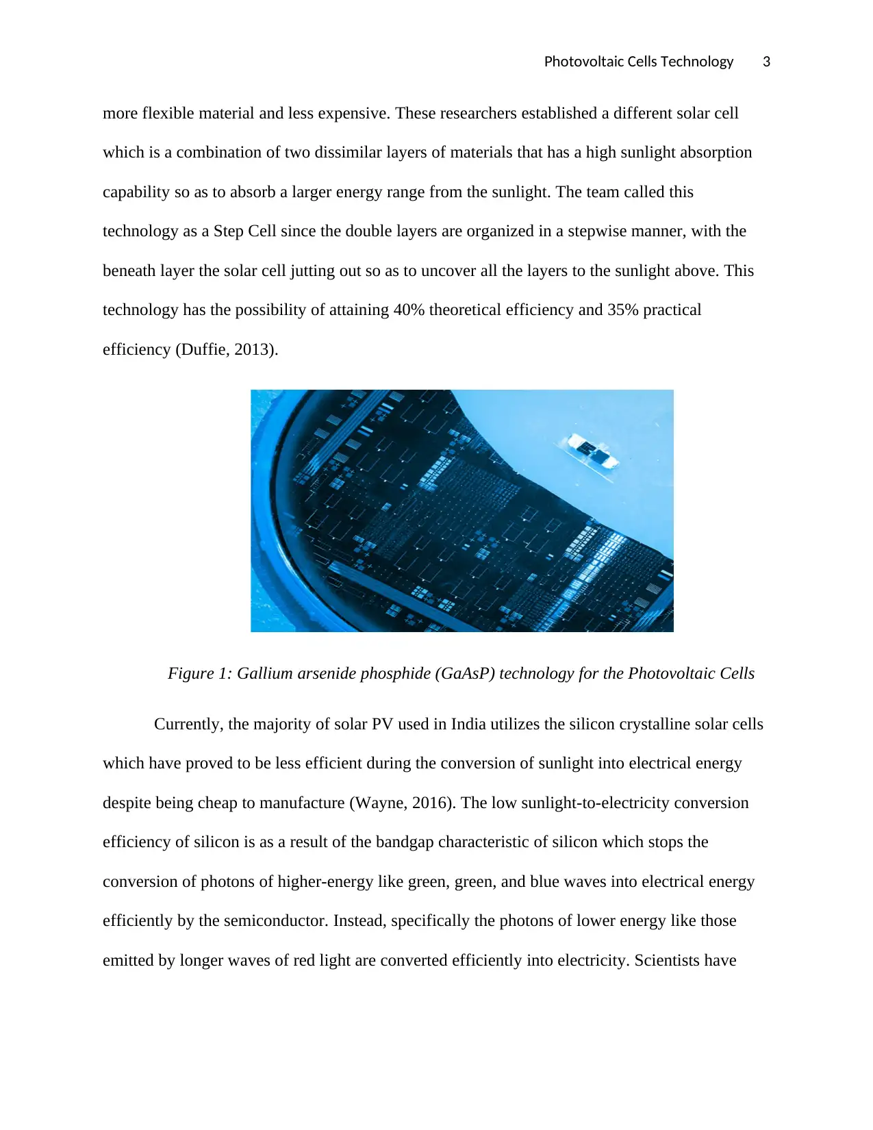
This research paper investigates the advancements in photovoltaic cell technology, with a specific focus on the potential of gallium arsenide phosphide (GaAsP) layering for enhancing solar energy efficiency in India. The paper highlights India's ambitious goals for solar energy generation and the need for cost-effective and efficient solar PV technologies. It delves into the limitations of traditional silicon crystalline solar cells and proposes the use of GaAsP nanoparticles to improve light absorption and energy conversion. The 'Step Cell' technology, involving a combination of GaAsP and silicon layers, is discussed as a promising approach to achieve higher theoretical and practical efficiencies. The research also addresses challenges related to the growth of GaAsP on silicon and the role of silicon germanium, ultimately suggesting a method for SiGe reuse to reduce manufacturing costs. The paper concludes by emphasizing the potential of this technology to bridge the gap between low-efficiency and high-efficiency solar PV applications in the Indian market. Desklib provides access to this paper along with numerous study tools and resources.
Document Page
Photovoltaic Cells Technology 1
NEW TECHNOLOGY USED IN PHOTOVOLTAIC CELL
A Research Paper on Energy By
Student’s Name
Name of the Professor
Institutional Affiliation
City/State
Year/Month/Day
tabler-icon-diamond-filled.svg

Paraphrase This Document

Need a fresh take? Get an instant paraphrase of this document with our AI Paraphraser
Document Page
Photovoltaic Cells Technology 2
INTRODUCTION
This research paper seeks to investigate the new technology used in the photovoltaic cell
which can be significant for India in specific. India stands at an installed capacity of solar energy
of approximately 2.9 GW as in 2014. However, the government seeks to scale up the solar
energy generation to a cumulative 100 GW by 2022 with major consideration being taken to the
generating skilled workforce, indigenous solar PV manufacturing, mass production, innovation
in low cost of manufacturing process, application of locally and new available materials, less
material consumption, and higher energy conversion efficiency of the solar PV. Researchers
have investigated on numerous ways in which the cost-effectiveness and efficiency of the solar
cell can be improved and some of these technologies can be effectively be used in India so as to
attain the targeted solar PV generation capacity (Boxwell, 2010).
A solar PV array is composed of numerous solar cells which individually converts the
radiant sunlight into electrical energy. The average efficiency of a normal solar cell is about
15%, which means that approximately 85% of the sunlight that hits the solar cells does not get
converted into electrical energy (Duffie, 2013). The current technologies that are currently being
developed or that have been improved from the current once seek to boost this efficiency to
improve the light captured by the solar PV and the solar energy converted. This research
proposes the light-sensitive nanoparticles such as layering gallium arsenide phosphide (GaAsP)
technology for the solar PV which a group of scientist disclosed at Masdar Institute of Science
and Technology who came up with this technology as an intractable tradeoff between cost and
efficiency of the solar PV (Chaturvedi, 2009).
In this technology of light-sensitive nanoparticles known as gallium arsenide phosphide
(GaAsP) technology are used since they are known to increase radiant light absorption and also
Document Page
Photovoltaic Cells Technology 3
more flexible material and less expensive. These researchers established a different solar cell
which is a combination of two dissimilar layers of materials that has a high sunlight absorption
capability so as to absorb a larger energy range from the sunlight. The team called this
technology as a Step Cell since the double layers are organized in a stepwise manner, with the
beneath layer the solar cell jutting out so as to uncover all the layers to the sunlight above. This
technology has the possibility of attaining 40% theoretical efficiency and 35% practical
efficiency (Duffie, 2013).
Figure 1: Gallium arsenide phosphide (GaAsP) technology for the Photovoltaic Cells
Currently, the majority of solar PV used in India utilizes the silicon crystalline solar cells
which have proved to be less efficient during the conversion of sunlight into electrical energy
despite being cheap to manufacture (Wayne, 2016). The low sunlight-to-electricity conversion
efficiency of silicon is as a result of the bandgap characteristic of silicon which stops the
conversion of photons of higher-energy like green, green, and blue waves into electrical energy
efficiently by the semiconductor. Instead, specifically the photons of lower energy like those
emitted by longer waves of red light are converted efficiently into electricity. Scientists have
Document Page
Photovoltaic Cells Technology 4
investigated numerous materials of the semiconductor so as to harness more higher-energy
photons of the sun such as gallium phosphide and gallium arsenide (Hough, 2011).
The solar cells of higher efficiency have been made by layering diverse materials of a
semiconductor such as gallium phosphide and gallium arsenide so as to attain attained higher
efficiencies compared to that of silicon so that every layer can be involved in the absorption of
diverse slice of electromagnetic spectrum. This proposed technology of solar PV is known as a
Step Cell and is made by gallium arsenide phosphide layering which is composed of a
semiconductor material which efficiently converts and absorbs photons of higher energy on a
solar cell of low cost (Mukerjee, 2011).
At the bottom step, there is an exposed layer of silicon. This design technology enables
the top layer of GaAsP to absorb the photos of higher energy such as the green, yellow, and blue
light leaving the layer of silicon at the bottom free to absorb photons of minor energy such as red
light from both the entire visible spectrum and also transmitted through the upper layer of the
Solar PV. The logic behind this arrangement is that when the top layer of GaAsP covered
completely the bottom layer of silicon, the photons of lower energy are absorbed by the silicon
gallium which is the substrate on which the GaAsP is grown making this arrangement of solar
cells to have a lower efficiency (Reddy, 2012).
Simulation-based on the results from the results from the experiment to determine the
geometrical configuration and optimal levels of the gallium arsenide phosphide (GaAsP)
technology which was conducted by Masdar Institute associated professor of computer science
and electrical engineering, Ammar Nayfeh, yielded a higher efficiency (Wayne, 2016). The
GaAsP was directly grown on the silicon germanium since the GaAsP cannot be directly grown
on silicon due to its crystal lattices significantly vary from that of silicon. The problem with the
tabler-icon-diamond-filled.svg

Paraphrase This Document

Need a fresh take? Get an instant paraphrase of this document with our AI Paraphraser
Document Page
Photovoltaic Cells Technology 5
silicon germanium under the layer of gallium arsenide phosphide is that silicon germanium
absorbs the light waves of lower energy before the sunlight reach the layer of silicon at the
bottom, and the silicon germanium is not involved in the conversion of these light waves of low
energy into the current (Roy, 2018).
This optical issue caused by the silicon germanium can be solved by the concept of the
step cell technology which enables different bands of energy absorption of silicon and gallium
arsenide phosphate. This technology of step cell resulted to a developed cell in which the
template of SiGe is re-used and removed, making a solar cell in which the tiles of GaAsP cells
are on topmost of the silicon cell directly. The step cell technology enables silicon germanium
reuse since the tiles of gallium arsenide phosphide cells can be undercut during the procedure of
transfer. The SiGe can be repeatedly reused and removed since the tandem cell is attached
together, rather than developed as a monolithic solar cell where every layer is developed into a
specific substrate. This reduced the cost of manufacturing significantly (Sivaram, 2018).
The addition of a single layer of the GaAsP can actually improve the efficiency of the
solar cell as well as the entire solar PV and also the cost of silicon germanium due to the unique
capability of etching away the SiGe and use it again over the process of manufacturing numerous
cells. The researchers have proved that this technology of the step cell can fit well in the current
market of the solar PV in India, between the low-efficiency and super high-efficiency
applications in industries (Solanki, 2015).
Conclusion
This research paper investigates the new technology used in the photovoltaic cell which
can be significant for India in specific. Researchers have investigated on numerous ways in
Document Page
Photovoltaic Cells Technology 6
which the cost-effectiveness and efficiency of the solar cell can be improved and some of these
technologies can be effectively be used in India so as to attain the targeted solar PV generation
capacity. This research proposes the light-sensitive nanoparticles such as layering gallium
arsenide phosphide (GaAsP) technology for the solar PV which a group of scientist unveiled at
Masdar Institute of Science and Technology who came up with this technology as an intractable
tradeoff between cost and efficiency of the solar PV. In this technology proposed for India, the
solar cells of higher efficiency have been developed by layering diverse materials of a
semiconductor such as gallium phosphide and gallium arsenide so as to attain attained higher
efficiencies compared to that of silicon so that every layer that is involved in the absorption of
diverse portion of electromagnetic spectrum.
Document Page
Photovoltaic Cells Technology 7
BIBLIOGRAPHY
Boxwell, M., 2010. Solar Electricity Handbook: A Simple, Practical Guide to Solar Energy - Designing and
Installing Photovoltaic Solar Electric Systems. Colorado: Greenstream Publishing.
Chaturvedi, P., 2009. Sustainable Energy Supply in Asia: Proceedings of the International Conference,
Asia Energy Vision 2020, Organised by the Indian Member Committee, World Energy Council Under the
Institution of Engineers (India). New Delhi: Concept Publishing Company.
Duffie, J., Duffie, A., 2013. Solar Engineering of Thermal Processes. Madison: John Wiley & Sons.
Hough, T., 2011. Trends in Solar Energy Research. Mumbai: Nova Publishers.
Mukherjee, K., Thakur, N., 2011. PHOTOVOLTAIC SYSTEMS: ANALYSIS AND DESIGN. New Delhi: PHI
Learning Pvt. Ltd.
Reddy, J., 2012. Solar Power Generation: Technology, New Concepts & Policy. Tirupathi: CRC Press.
Roy, N., Bose, D., 2018. Photovoltaic Science and Technology. Cambridge University: Cambridge
University Press.
Sivaram, V., 2018. Taming the Sun: Innovations to Harness Solar Energy and Power the Planet. California:
MIT Press.
Solanki, C., 2015. Solar Photovoltaics: Fundamentals, Technologies And Applications. Bombay: PHI
Learning Pvt. Ltd.
Wayne, G., Isaac, W., 2016. Environmental Sustainability and Climate Change Adaptation Strategies.
New York: IGI Global.
chevron_up_icon
1 out of 7
circle_padding
hide_on_mobile
zoom_out_icon
[object Object]