Embedded Systems Lab Report: PIC Development and E-Block System
VerifiedAdded on 2020/04/15
|62
|8987
|48
Report
AI Summary
This report presents a series of lab exercises focused on embedded systems, utilizing the PIC16F877A microcontroller and the Matrix E-Block system. The labs cover a range of topics, including system orientation, programming applications, microcontroller family orientation, and practical experiments involving input/output control, LCD display animation, timer modules, and interrupt handling. The report details the purpose, procedures, and outcomes of each exercise, providing insights into the functionality of various components such as sensor boards, LED boards, switch boards, and the PIC micro programmer. It emphasizes the use of Flowcode for programming and the capabilities of the E-Block system for rapid prototyping and educational purposes. The report also includes circuit diagrams and key features of the hardware components, offering a comprehensive overview of the embedded systems development process.

Paraphrase This Document
Need a fresh take? Get an instant paraphrase of this document with our AI Paraphraser

EMBEDDED SYSTEMS

Table of Contents
Lab - 1...................................................................................................................................................3
Exercise-1 Matrix E-Block System Orientation...................................................................................3
Purpose.........................................................................................................................................3
Procedure.....................................................................................................................................3
Key Features..................................................................................................................................10
Exercise No.2: PPP Programmer Application Orientation................................................................17
Purpose.......................................................................................................................................17
Procedure...................................................................................................................................17
Results........................................................................................................................................20
Exercise No.3: Family Orientation of Microchip PIC MCU................................................................22
Purpose.......................................................................................................................................22
Procedure...................................................................................................................................22
Results........................................................................................................................................26
Conclusion.......................................................................................................................................27
Lab -2..................................................................................................................................................27
Exercise 1 – PORTB timed lighting sequence...................................................................................28
Aim.............................................................................................................................................28
Procedure...................................................................................................................................28
Outcomes....................................................................................................................................30
The...........................................................................................................................................30
Exercise 2 Combining input and output...........................................................................................30
Aim.............................................................................................................................................30
Procedure...................................................................................................................................30
Outcomes....................................................................................................................................32
Lab - 3.................................................................................................................................................32
Exercise-1........................................................................................................................................32
Aim.............................................................................................................................................32
Procedure...................................................................................................................................32
Exercise -2 Animating using the LCD display....................................................................................35
Aim.............................................................................................................................................35
Outcomes....................................................................................................................................36
Exercise 3 - Displaying numerical information.................................................................................36
Aim.............................................................................................................................................37
Procedure...................................................................................................................................37
⊘ This is a preview!⊘
Do you want full access?
Subscribe today to unlock all pages.
Trusted by 1+ million students worldwide
Outcomes....................................................................................................................................43
Lab-4..................................................................................................................................................43
Exercise-1 create a simple delay using Timer0 module...................................................................43
Aim.............................................................................................................................................43
Procedure...................................................................................................................................43
Outcomes....................................................................................................................................45
Exercise-2 creating longer delay......................................................................................................45
Aim.............................................................................................................................................45
Procedure...................................................................................................................................45
Outcomes....................................................................................................................................47
Exercise-3 creating a one second delay using Timer0 module.........................................................48
Aim.............................................................................................................................................48
Procedure...................................................................................................................................48
Outcomes....................................................................................................................................50
Exercise-4 creating a variable delay.................................................................................................50
Aim.............................................................................................................................................50
Procedure...................................................................................................................................50
Outcomes....................................................................................................................................51
Lab -5..................................................................................................................................................51
Exercise-1 Creating precise delays using interrupts.........................................................................51
Aim.............................................................................................................................................52
Procedure...................................................................................................................................52
Outcomes....................................................................................................................................53
Exercise-2 creating precise delays using interrupts.........................................................................53
Aim.............................................................................................................................................53
Procedure...................................................................................................................................53
Outcomes....................................................................................................................................54
Exercise-3 adding background code functionality...........................................................................54
Aim.............................................................................................................................................54
Procedure...................................................................................................................................54
Outcomes....................................................................................................................................56
Exercise-4 servicing multiple interrupts...........................................................................................56
Aim.............................................................................................................................................56
Procedure...................................................................................................................................56
Outcomes....................................................................................................................................57
References..........................................................................................................................................58
Paraphrase This Document
Need a fresh take? Get an instant paraphrase of this document with our AI Paraphraser
Lab - 1
Exercise-1 Matrix E-Block System Orientation
Purpose
This is a lab work designed to orientate with the PIC development system. For the
PIC16F877A microcontroller, the PIC development system can be utilised for developing,
building and debugging the embedded C projects. The PIC development system contains the
required hardware and software tools to accomplish the needs.
Procedure
The small circuit boards called E-Blocks consists a block of electronics, which is
generally available in the embedded system. It also contains additional 50 separate circuit
boards, which have device programmers ranging from both simple and complicated LED
boards. Further, it contains TCP/IP and Bluetooth. The E-blocks could be snapped together
for forming large types of systems, which can be used for teaching/learning electronics and
for the rapid prototyping of complex electronic systems.
Separate ranges of complementary software, curriculum, sensors, and applications
information are available. The E-blocks tends to help various programmable devices from the
PIC, AVR, dsPIC, ARM, PIC24 and the Altera FPGA families. Communications standards
support includes SPI, RS232, I2C, TCP/IP, USB, LIN, CAN, Bluetooth, GSM, GPS, ZigBee,
RFID, MIDI, IrDA, RF(ISM), RC5, RS485 and much more.
This E-block contains a variable resistor and a simple light sensor which can be used
for simple analogue experiments. It also contains sockets which allow users to interface to
our range of more than 30 professional sensors including pH, temperature, distance, g etc..
Key Characteristics
1) It has Flow code macro.
2) Compatible E-blocks
3) It has on-board potential divider.
4) Greater than 29 sensors are supported.
5) It has on-board light sensor.

Sensor Board
Description of the Circuit
1) The circuit contains 9-way D-type plug.
2) It has patch system.
3) It contains link blocks.
4) It comprises of screw terminals.
5) It also consists of Photodiode.
6) Then, it has external digital sensor ("New/Popular PIC10 MCU Products -
Microchip Technology Inc", 2017).
7) Next, it contains external analogue sensor.
8) Further, it has potentiometer, which helps to simulate the differing analogue
voltage.
Key Features of the Sensor Board
1) The sensor board is compatible with E-blocks.
2) It has complete range of external sensors, then Downstream D-type connector and
On-board photodiode.
3) In the E-blocks range, the sensor board has compatibility with the majority of the
I/O ports.
4) Flow code helps in developing the programming code.
⊘ This is a preview!⊘
Do you want full access?
Subscribe today to unlock all pages.
Trusted by 1+ million students worldwide
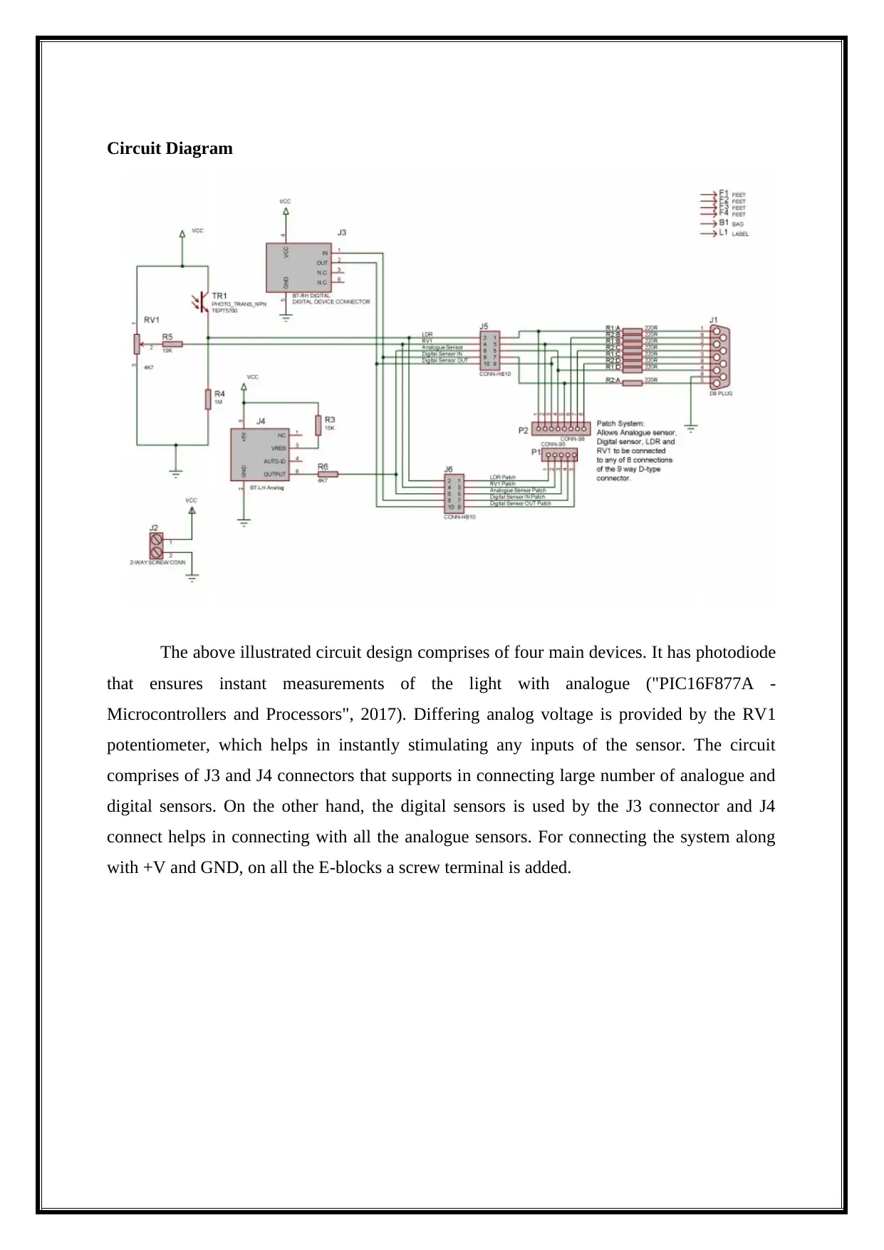
Circuit Diagram
The above illustrated circuit design comprises of four main devices. It has photodiode
that ensures instant measurements of the light with analogue ("PIC16F877A -
Microcontrollers and Processors", 2017). Differing analog voltage is provided by the RV1
potentiometer, which helps in instantly stimulating any inputs of the sensor. The circuit
comprises of J3 and J4 connectors that supports in connecting large number of analogue and
digital sensors. On the other hand, the digital sensors is used by the J3 connector and J4
connect helps in connecting with all the analogue sensors. For connecting the system along
with +V and GND, on all the E-blocks a screw terminal is added.
Paraphrase This Document
Need a fresh take? Get an instant paraphrase of this document with our AI Paraphraser
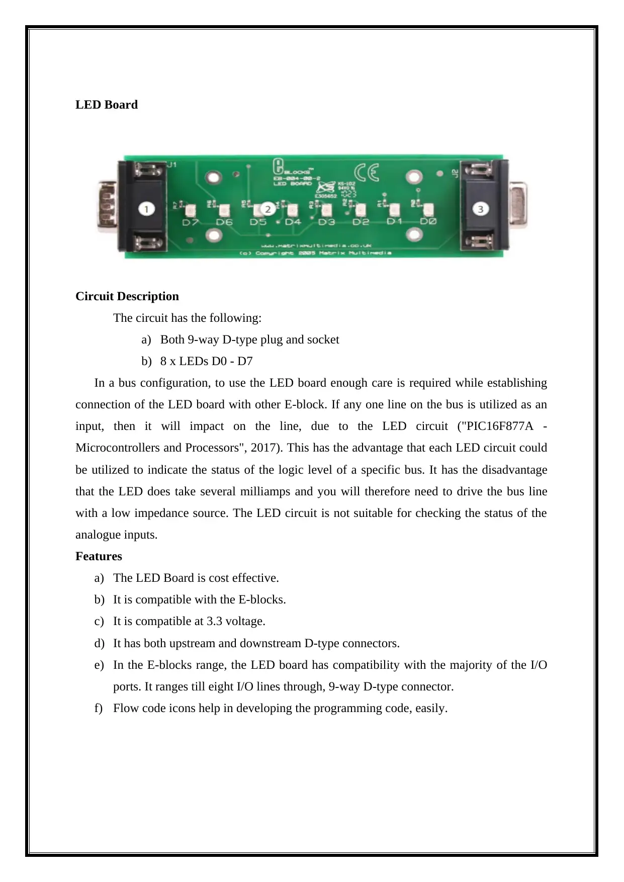
LED Board
Circuit Description
The circuit has the following:
a) Both 9-way D-type plug and socket
b) 8 x LEDs D0 - D7
In a bus configuration, to use the LED board enough care is required while establishing
connection of the LED board with other E-block. If any one line on the bus is utilized as an
input, then it will impact on the line, due to the LED circuit ("PIC16F877A -
Microcontrollers and Processors", 2017). This has the advantage that each LED circuit could
be utilized to indicate the status of the logic level of a specific bus. It has the disadvantage
that the LED does take several milliamps and you will therefore need to drive the bus line
with a low impedance source. The LED circuit is not suitable for checking the status of the
analogue inputs.
Features
a) The LED Board is cost effective.
b) It is compatible with the E-blocks.
c) It is compatible at 3.3 voltage.
d) It has both upstream and downstream D-type connectors.
e) In the E-blocks range, the LED board has compatibility with the majority of the I/O
ports. It ranges till eight I/O lines through, 9-way D-type connector.
f) Flow code icons help in developing the programming code, easily.
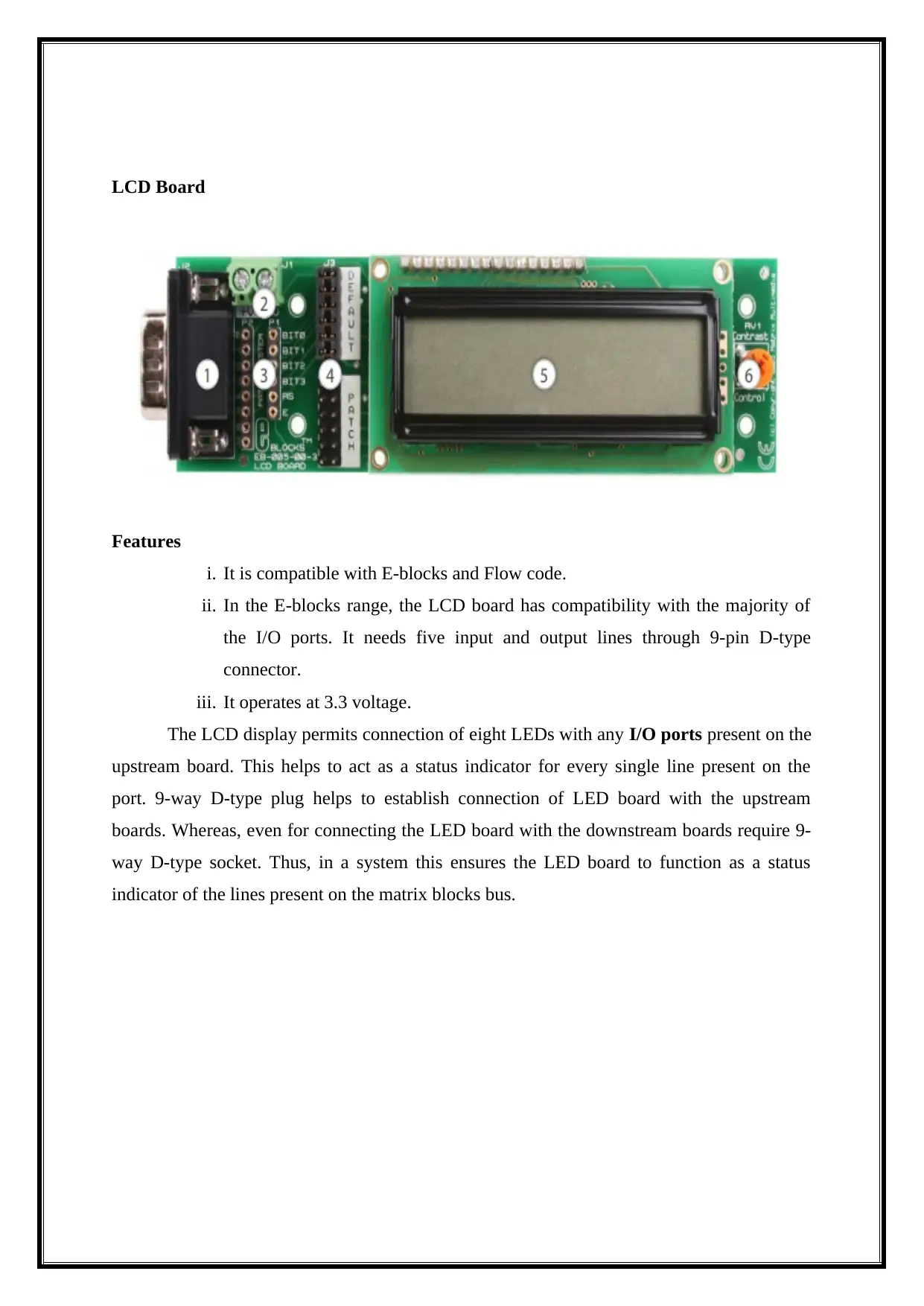
LCD Board
Features
i. It is compatible with E-blocks and Flow code.
ii. In the E-blocks range, the LCD board has compatibility with the majority of
the I/O ports. It needs five input and output lines through 9-pin D-type
connector.
iii. It operates at 3.3 voltage.
The LCD display permits connection of eight LEDs with any I/O ports present on the
upstream board. This helps to act as a status indicator for every single line present on the
port. 9-way D-type plug helps to establish connection of LED board with the upstream
boards. Whereas, even for connecting the LED board with the downstream boards require 9-
way D-type socket. Thus, in a system this ensures the LED board to function as a status
indicator of the lines present on the matrix blocks bus.
⊘ This is a preview!⊘
Do you want full access?
Subscribe today to unlock all pages.
Trusted by 1+ million students worldwide
Circuit Diagram
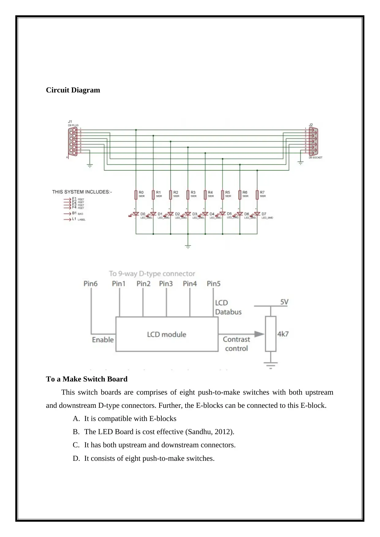
To a Make Switch Board
This switch boards are comprises of eight push-to-make switches with both upstream
and downstream D-type connectors. Further, the E-blocks can be connected to this E-block.
A. It is compatible with E-blocks
B. The LED Board is cost effective (Sandhu, 2012).
C. It has both upstream and downstream connectors.
D. It consists of eight push-to-make switches.
Paraphrase This Document
Need a fresh take? Get an instant paraphrase of this document with our AI Paraphraser
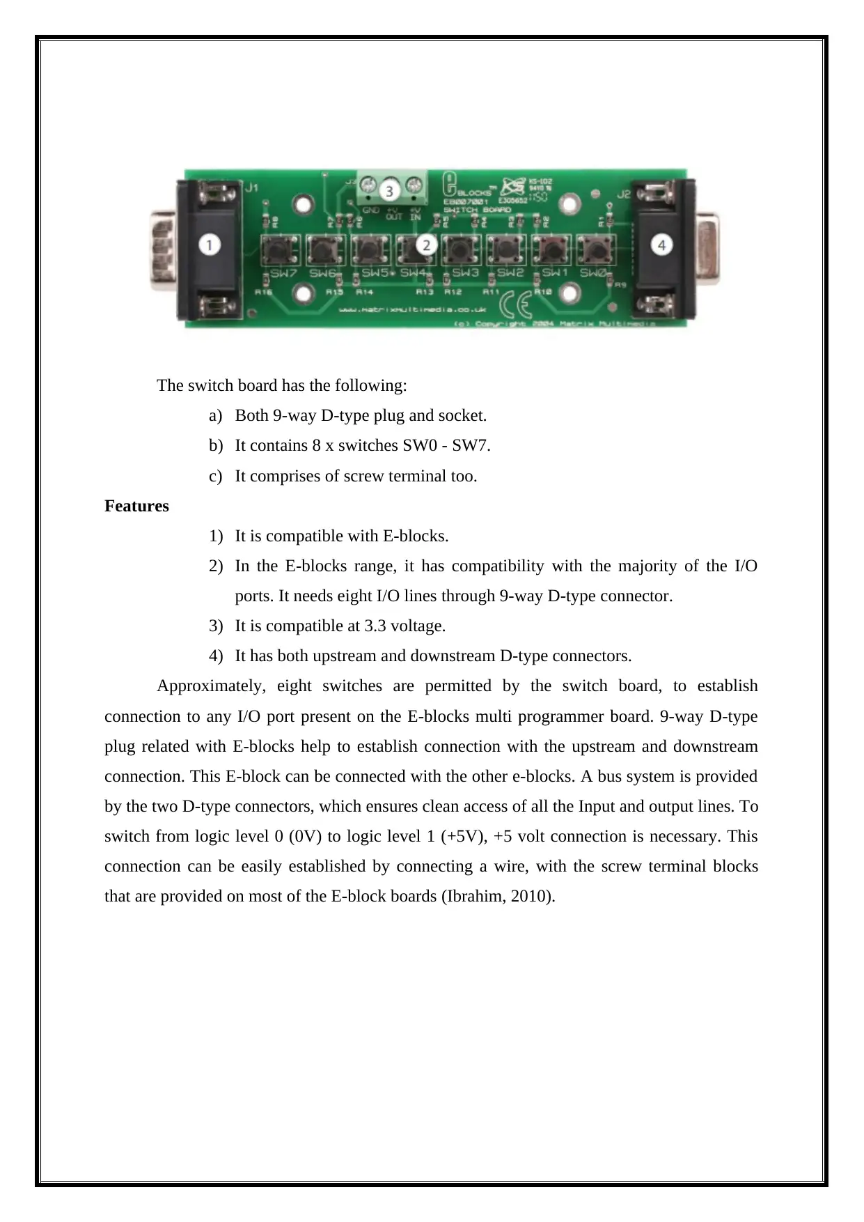
The switch board has the following:
a) Both 9-way D-type plug and socket.
b) It contains 8 x switches SW0 - SW7.
c) It comprises of screw terminal too.
Features
1) It is compatible with E-blocks.
2) In the E-blocks range, it has compatibility with the majority of the I/O
ports. It needs eight I/O lines through 9-way D-type connector.
3) It is compatible at 3.3 voltage.
4) It has both upstream and downstream D-type connectors.
Approximately, eight switches are permitted by the switch board, to establish
connection to any I/O port present on the E-blocks multi programmer board. 9-way D-type
plug related with E-blocks help to establish connection with the upstream and downstream
connection. This E-block can be connected with the other e-blocks. A bus system is provided
by the two D-type connectors, which ensures clean access of all the Input and output lines. To
switch from logic level 0 (0V) to logic level 1 (+5V), +5 volt connection is necessary. This
connection can be easily established by connecting a wire, with the screw terminal blocks
that are provided on most of the E-block boards (Ibrahim, 2010).
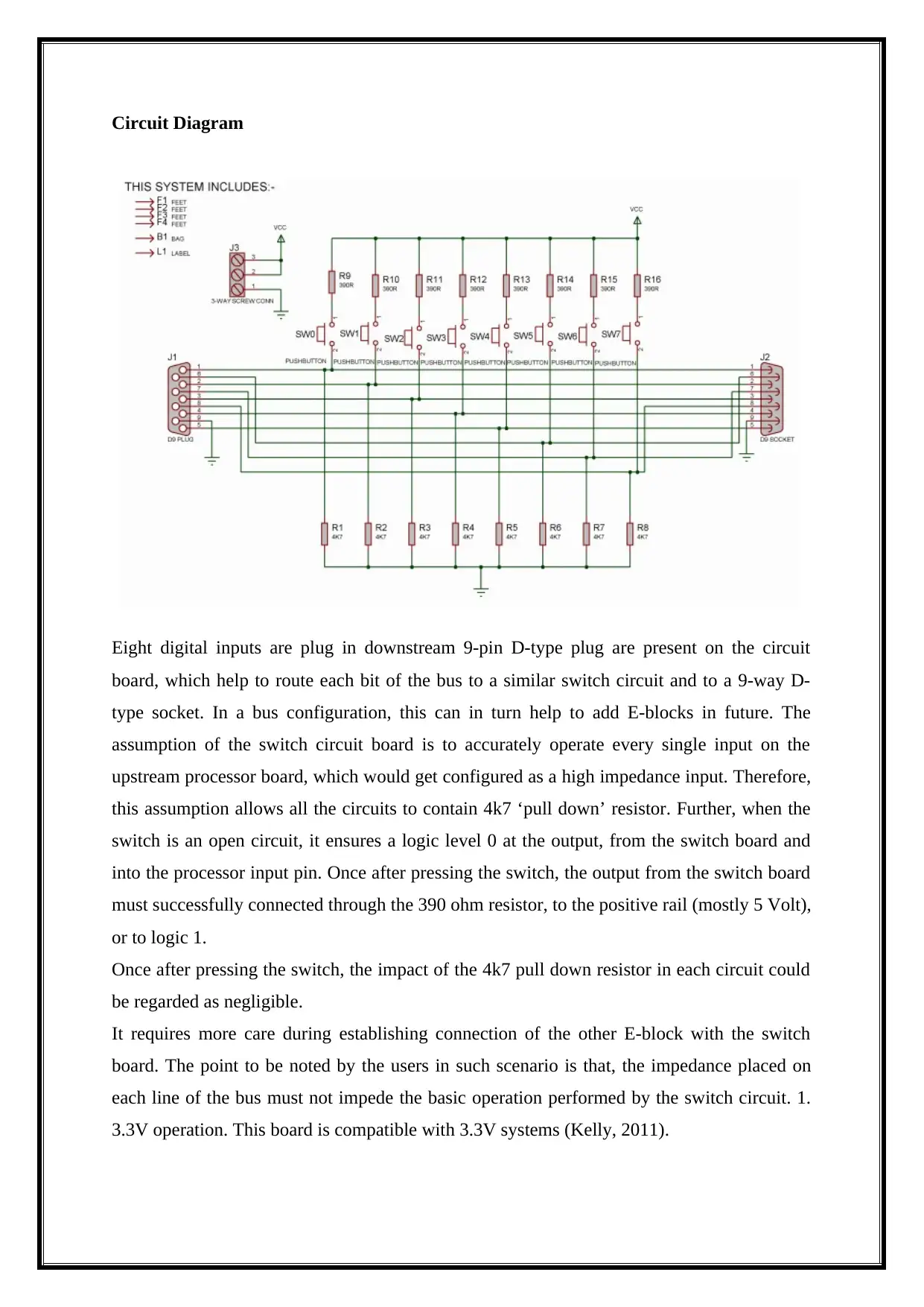
Circuit Diagram
Eight digital inputs are plug in downstream 9-pin D-type plug are present on the circuit
board, which help to route each bit of the bus to a similar switch circuit and to a 9-way D-
type socket. In a bus configuration, this can in turn help to add E-blocks in future. The
assumption of the switch circuit board is to accurately operate every single input on the
upstream processor board, which would get configured as a high impedance input. Therefore,
this assumption allows all the circuits to contain 4k7 ‘pull down’ resistor. Further, when the
switch is an open circuit, it ensures a logic level 0 at the output, from the switch board and
into the processor input pin. Once after pressing the switch, the output from the switch board
must successfully connected through the 390 ohm resistor, to the positive rail (mostly 5 Volt),
or to logic 1.
Once after pressing the switch, the impact of the 4k7 pull down resistor in each circuit could
be regarded as negligible.
It requires more care during establishing connection of the other E-block with the switch
board. The point to be noted by the users in such scenario is that, the impedance placed on
each line of the bus must not impede the basic operation performed by the switch circuit. 1.
3.3V operation. This board is compatible with 3.3V systems (Kelly, 2011).
⊘ This is a preview!⊘
Do you want full access?
Subscribe today to unlock all pages.
Trusted by 1+ million students worldwide
1 out of 62


Your All-in-One AI-Powered Toolkit for Academic Success.
+13062052269
info@desklib.com
Available 24*7 on WhatsApp / Email
![[object Object]](/_next/static/media/star-bottom.7253800d.svg)
Unlock your academic potential
Copyright © 2020–2026 A2Z Services. All Rights Reserved. Developed and managed by ZUCOL.