EE201: Power Amplifier Design and Simulation Project
VerifiedAdded on 2022/08/11
|27
|3863
|37
Project
AI Summary
This project details the design and simulation of a class A common emitter power amplifier using an NPN transistor (BC109). The report starts with an introduction to amplifiers, including frequency response, gain calculations (voltage and power), and H-parameter models. It then covers the design process, focusing on finding the collector load resistance, determining the DC operating point, and calculating the biasing resistor values (R1 and R2) using voltage divider biasing. The project also explores modifications to Class B and Class AB amplifiers. The design includes detailed calculations and analysis, including the determination of the DC load line, input power, and biasing current. The report culminates with simulation results and analysis, providing a comprehensive understanding of power amplifier design principles.
1
Student
Instructor
Title
POWER AMPLIFIERS DESIGN AND SIMULATION.
Date
Student
Instructor
Title
POWER AMPLIFIERS DESIGN AND SIMULATION.
Date
Paraphrase This Document
Need a fresh take? Get an instant paraphrase of this document with our AI Paraphraser
2
Table of Contents
1: INTRODUCTION.....................................................................................................................3
1.1: Finding Current Gain Ai.......................................................................................................5
1.2: Finding the Input Resistance.................................................................................................6
1.3: Finding Voltage Gain AV .....................................................................................................7
2: DESIGNING OF THE COMMON EMITTER POWER AMPLIFIER..............................9
2.1: Finding suitable collector load resistance of the circuit........................................................9
2.2: Finding the D.C operating point of the amplifier on the DC load line...............................10
2.3: Finding biasing resistor R1 and R2.....................................................................................15
2.4: Modification into Class B Amplifier..................................................................................18
2.5: Modification into Class AB Amplifier...............................................................................18
2.6: Modification into Class C Amplifier..................................................................................19
3: SIMULATION.........................................................................................................................21
4: RESULTS AND ANALYSIS..................................................................................................23
5: CONCLUSION........................................................................................................................25
6: REFERNCES...........................................................................................................................26
3
1: INTRODUCTION.
The project entails designing of class A amplifier using NPN transistor. The transistor naturally
operates as an amplifier in the active region where the collector current is linearly dependent on
the base current (ElProCus, 2020). Weak input signal at the base terminal of the transistor is
amplified when the base emitter junction of the transistor is forward biased. The polarity of the
input signal does not however, affects the biasing of the transistor (Tutorialspoint.com, 2018).
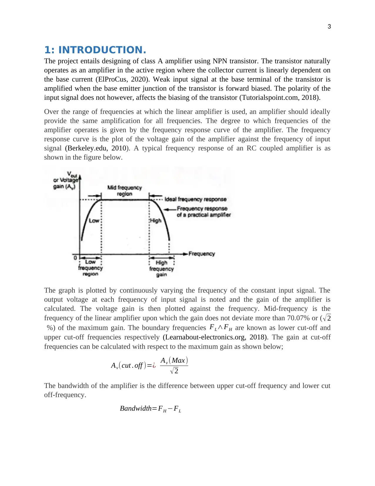
Over the range of frequencies at which the linear amplifier is used, an amplifier should ideally
provide the same amplification for all frequencies. The degree to which frequencies of the
amplifier operates is given by the frequency response curve of the amplifier. The frequency
response curve is the plot of the voltage gain of the amplifier against the frequency of input
signal (Berkeley.edu, 2010). A typical frequency response of an RC coupled amplifier is as
shown in the figure below.
The graph is plotted by continuously varying the frequency of the constant input signal. The
output voltage at each frequency of input signal is noted and the gain of the amplifier is
calculated. The voltage gain is then plotted against the frequency. Mid-frequency is the
frequency of the linear amplifier upon which the gain does not deviate more than 70.07% or ( √ 2
%) of the maximum gain. The boundary frequencies FL∧FH are known as lower cut-off and
upper cut-off frequencies respectively (Learnabout-electronics.org, 2018). The gain at cut-off
frequencies can be calculated with respect to the maximum gain as shown below;
Av(cut . off )=¿ Av (Max)
√2
The bandwidth of the amplifier is the difference between upper cut-off frequency and lower cut
off-frequency.
Bandwidth=FH −FL
1: INTRODUCTION.
The project entails designing of class A amplifier using NPN transistor. The transistor naturally
operates as an amplifier in the active region where the collector current is linearly dependent on
the base current (ElProCus, 2020). Weak input signal at the base terminal of the transistor is
amplified when the base emitter junction of the transistor is forward biased. The polarity of the
input signal does not however, affects the biasing of the transistor (Tutorialspoint.com, 2018).
Over the range of frequencies at which the linear amplifier is used, an amplifier should ideally
provide the same amplification for all frequencies. The degree to which frequencies of the
amplifier operates is given by the frequency response curve of the amplifier. The frequency
response curve is the plot of the voltage gain of the amplifier against the frequency of input
signal (Berkeley.edu, 2010). A typical frequency response of an RC coupled amplifier is as
shown in the figure below.
The graph is plotted by continuously varying the frequency of the constant input signal. The
output voltage at each frequency of input signal is noted and the gain of the amplifier is
calculated. The voltage gain is then plotted against the frequency. Mid-frequency is the
frequency of the linear amplifier upon which the gain does not deviate more than 70.07% or ( √ 2
%) of the maximum gain. The boundary frequencies FL∧FH are known as lower cut-off and
upper cut-off frequencies respectively (Learnabout-electronics.org, 2018). The gain at cut-off
frequencies can be calculated with respect to the maximum gain as shown below;
Av(cut . off )=¿ Av (Max)
√2
The bandwidth of the amplifier is the difference between upper cut-off frequency and lower cut
off-frequency.
Bandwidth=FH −FL
⊘ This is a preview!⊘
Do you want full access?
Subscribe today to unlock all pages.
Trusted by 1+ million students worldwide
4
The amplifier amplifies properly within range of frequencies in the bandwidth. A good audio
amplifier must have bandwidth from 20 Hz to 20 kHz because that is the frequency range which
is audible.
The gain of the amplifier is the ratio of output power to input power. Gain can also be given by
the ratio of output voltage to input voltage as shown on the equation below.
Av=V out
V ¿
Or
Ap = Pout
P¿
Voltage gain of the amplifier can also be given in Decibels as shown in the expression below.
Voltage gain∈dB=20 log Av
Also, the power gain in Decibel is given by;
Power gain∈dB=10 log A p
When Av is greater than one, the dB gain is positive and when it is less than one, the dB gain is
negative. The negative and positive signs of dB indicate the amplification and attenuation
respectively.
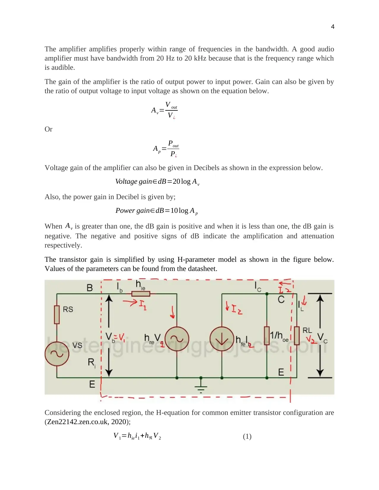
The transistor gain is simplified by using H-parameter model as shown in the figure below.
Values of the parameters can be found from the datasheet.
Considering the enclosed region, the H-equation for common emitter transistor configuration are
(Zen22142.zen.co.uk, 2020);
V 1=hie i1 +hℜ V 2 (1)
The amplifier amplifies properly within range of frequencies in the bandwidth. A good audio
amplifier must have bandwidth from 20 Hz to 20 kHz because that is the frequency range which
is audible.
The gain of the amplifier is the ratio of output power to input power. Gain can also be given by
the ratio of output voltage to input voltage as shown on the equation below.
Av=V out
V ¿
Or
Ap = Pout
P¿
Voltage gain of the amplifier can also be given in Decibels as shown in the expression below.
Voltage gain∈dB=20 log Av
Also, the power gain in Decibel is given by;
Power gain∈dB=10 log A p
When Av is greater than one, the dB gain is positive and when it is less than one, the dB gain is
negative. The negative and positive signs of dB indicate the amplification and attenuation
respectively.
The transistor gain is simplified by using H-parameter model as shown in the figure below.
Values of the parameters can be found from the datasheet.
Considering the enclosed region, the H-equation for common emitter transistor configuration are
(Zen22142.zen.co.uk, 2020);
V 1=hie i1 +hℜ V 2 (1)
Paraphrase This Document
Need a fresh take? Get an instant paraphrase of this document with our AI Paraphraser
5
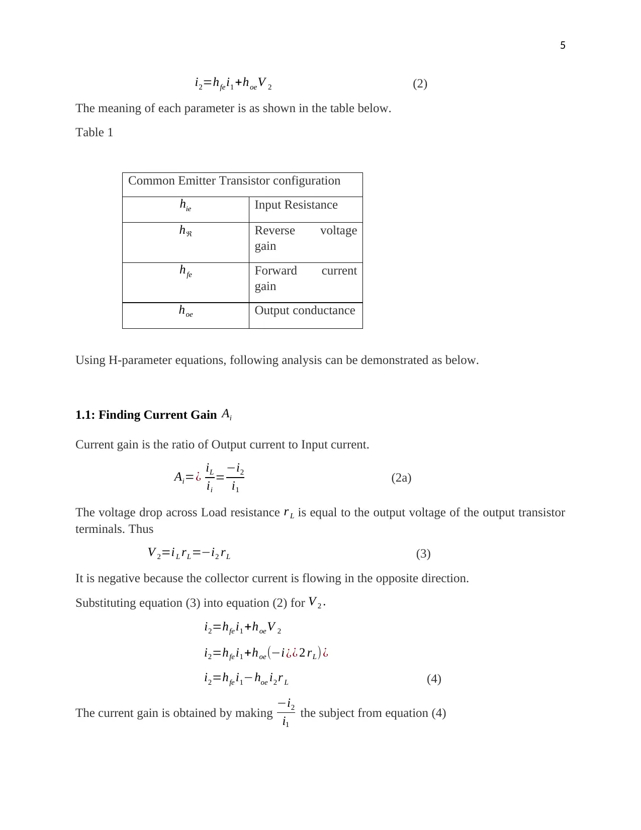
i2=hfei1 +hoeV 2 (2)
The meaning of each parameter is as shown in the table below.
Table 1
Common Emitter Transistor configuration
hie Input Resistance
hℜ Reverse voltage
gain
hfe Forward current
gain
hoe Output conductance
Using H-parameter equations, following analysis can be demonstrated as below.
1.1: Finding Current Gain Ai
Current gain is the ratio of Output current to Input current.
Ai=¿ iL
ii
=−i2
i1
(2a)
The voltage drop across Load resistance r L is equal to the output voltage of the output transistor
terminals. Thus
V 2=iL rL=−i2 rL (3)
It is negative because the collector current is flowing in the opposite direction.
Substituting equation (3) into equation (2) for V 2 .
i2=hfe i1 +hoe V 2
i2=hfe i1 +hoe (−i¿¿ 2 rL)¿
i2=hfe i1−hoe i2 r L (4)
The current gain is obtained by making −i2
i1
the subject from equation (4)
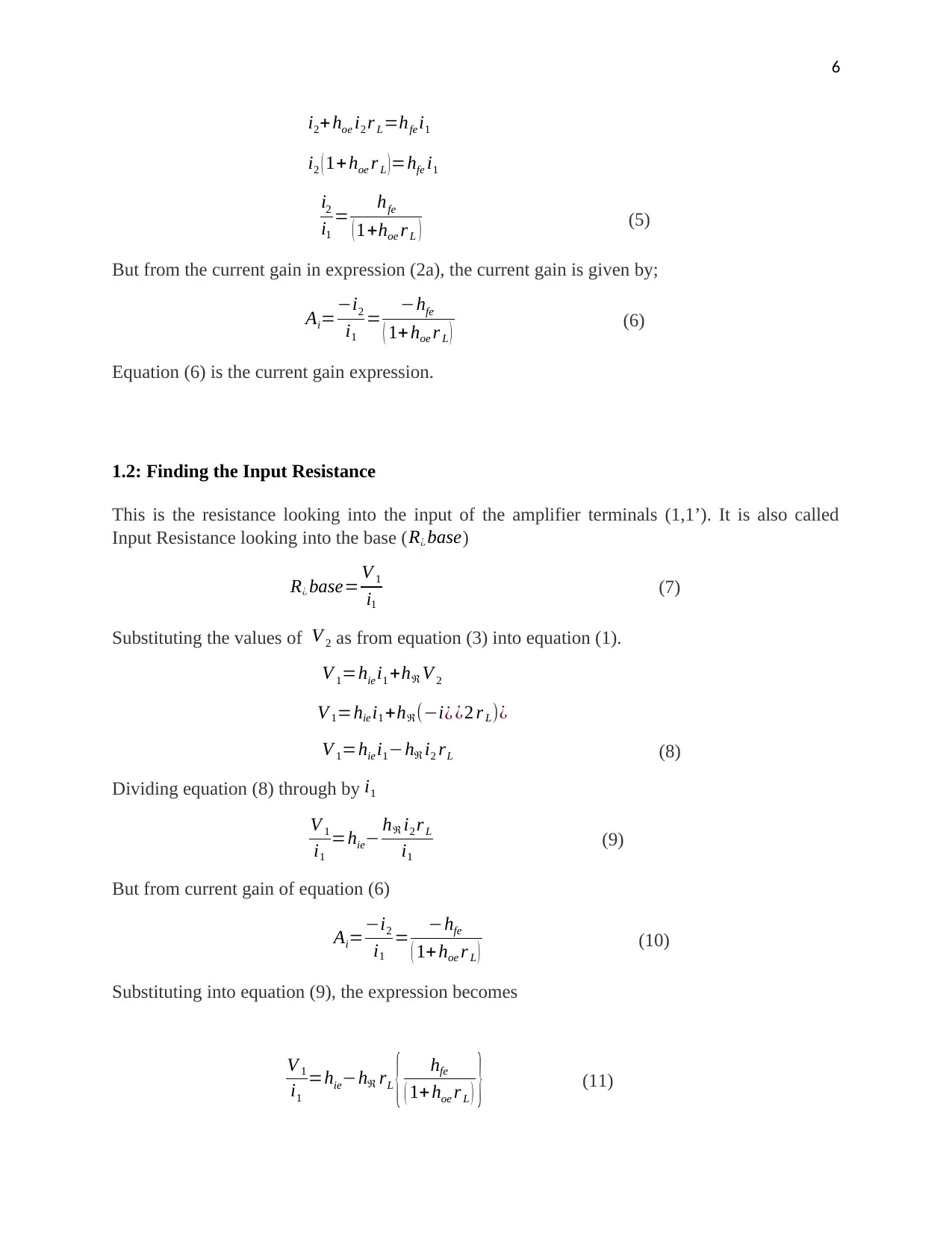
6
i2+ hoe i2 r L=hfe i1
i2 ( 1+hoe r L ) =hfe i1
i2
i1
= hfe
( 1+hoe r L ) (5)
But from the current gain in expression (2a), the current gain is given by;
Ai=−i2
i1
= −hfe
( 1+ hoe r L ) (6)
Equation (6) is the current gain expression.
1.2: Finding the Input Resistance
This is the resistance looking into the input of the amplifier terminals (1,1’). It is also called
Input Resistance looking into the base ( R¿ base)
R¿ base= V 1
i1
(7)
Substituting the values of V 2 as from equation (3) into equation (1).
V 1=hie i1 +hℜ V 2
V 1=hie i1 +hℜ(−i¿ ¿2 r L)¿
V 1=hie i1−hℜ i2 rL (8)
Dividing equation (8) through by i1
V 1
i1
=hie− hℜ i2 r L
i1
(9)
But from current gain of equation (6)
Ai=−i2
i1
= −hfe
( 1+ hoe r L ) (10)
Substituting into equation (9), the expression becomes
V 1
i1
=hie−hℜ rL { hfe
( 1+ hoe r L ) } (11)
⊘ This is a preview!⊘
Do you want full access?
Subscribe today to unlock all pages.
Trusted by 1+ million students worldwide
7
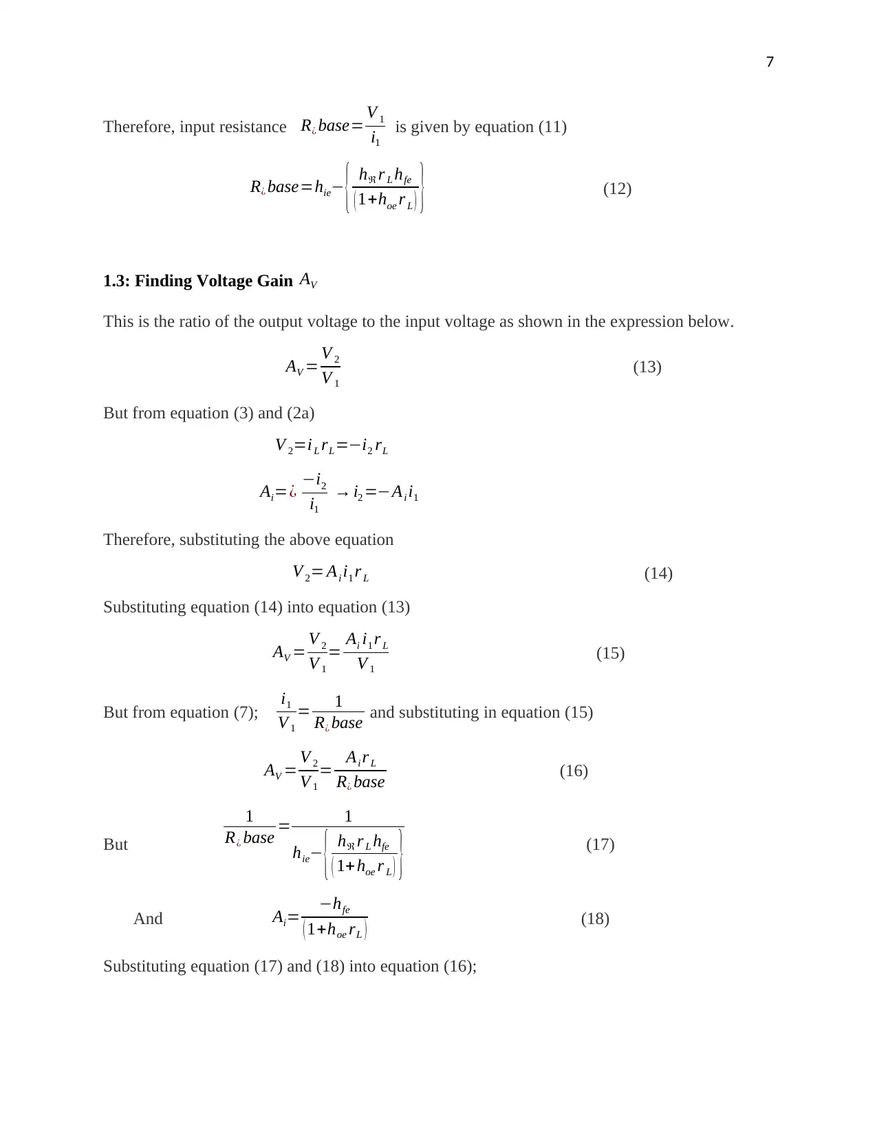
Therefore, input resistance R¿ base= V 1
i1
is given by equation (11)
R¿ base=hie− { hℜ r L hfe
( 1+hoe r L ) } (12)
1.3: Finding Voltage Gain AV
This is the ratio of the output voltage to the input voltage as shown in the expression below.
AV = V 2
V 1
(13)
But from equation (3) and (2a)
V 2=iL rL=−i2 rL
Ai=¿ −i2
i1
→ i2 =−Ai i1
Therefore, substituting the above equation
V 2= Ai i1 r L (14)
Substituting equation (14) into equation (13)
AV = V 2
V 1
= Ai i1 r L
V 1
(15)
But from equation (7); i1
V 1
= 1
R¿ base and substituting in equation (15)
AV = V 2
V 1
= Ai r L
R¿ base (16)
But
1
R¿ base = 1
hie− { hℜ r L hfe
( 1+ hoe r L ) } (17)
And Ai= −hfe
( 1+hoe rL ) (18)
Substituting equation (17) and (18) into equation (16);
Paraphrase This Document
Need a fresh take? Get an instant paraphrase of this document with our AI Paraphraser
8
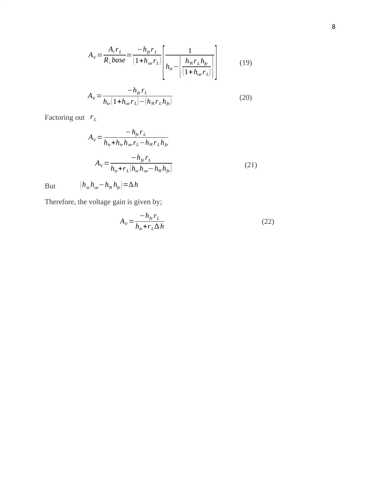
AV = Ai r L
R¿ base = −hfe r L
( 1+hoe rL )
[ 1
hie − { hℜ r L hfe
( 1+ hoe r L ) } ] (19)
AV = −hfe rL
hie ( 1+hoe r L ) − ( hℜ r L hfe ) (20)
Factoring out r L
AV = −hfe r L
hie +hie hoe rL−hℜ r L hfe
AV = −hfe rL
hie +r L ( hie hoe−hℜ hfe ) (21)
But ( hie hoe−hℜ hfe ) =∆ h
Therefore, the voltage gain is given by;
AV = −hfe rL
hie +r L ∆ h (22)
9
2: DESIGNING OF THE COMMON EMITTER POWER
AMPLIFIER.
The amplifier was designed by finding suitable parameters with regard to the desired operating
point. The design was done both in A.C and D.C analysis.
2.1: Finding suitable collector load resistance of the circuit.
The voltage gain and sinusoidal input voltage of the transistor power amplifier to be designed
has been specified in table 2 below.
Table 2
AV 5
v¿ 0.2 V p− p
Voltage gain the ratio of output voltage to the input sinusoidal voltage that is applied at the base
terminal of the transistor.
AV = vout
v¿
(23)
Using H-parameter, the voltage gain as in equation (22) was found to be;’
AV = −hfe rL
hie +r L ( hie hoe−hℜ hfe ) (24)
From the data sheet, H-parameters of the BC109 transistor is as shown in table (3) below
(Kitronik.co.uk, 2020)
Table 3
Common Emitter Transistor configuration
hie 5.5 kΩ
hℜ 3 ×10⁻⁴
hfe 370
hoe 30 μS
⊘ This is a preview!⊘
Do you want full access?
Subscribe today to unlock all pages.
Trusted by 1+ million students worldwide
10
With parameters in table (3), the values in equation (25) can be substituted as demonstrated
below.
−5=¿ − ( 370 ) rL
( 5.5 kΩ ) +r L { ( 5.5 kΩ ×30 μS ) − ( 3 ×10−4 ×370 ) } (26)
Simplifying the equation;
5=¿ ( 370 ) r L
( 5500Ω ) + rL { ( 5.5 Ω× 30 S × 10−3 ) − ( 3 ×10−4 × 370 ) } (27)
5=¿ ( 370 ) r L
( 5500Ω )+rL {0.054 } (28)
Making load resistance the subject;
5 ( ( 5500 Ω ) +r L { 0.054 } )= ( 370 ) r L (29)
27500= ( 369.946 ) rL (30)
Therefore, the load resistance at the collector terminal is;
r L= 27500
369.946 =74.33 Ω (31)
This load resistance can also be denoted as;
r L=RC=74.33 Ω
2.2: Finding the D.C operating point of the amplifier on the DC load line.
In this project, voltage divider biasing was preferred. The trade-off of this type of biasing over
the other discussed methods is that there is reduced effects of temperature on current gain, β.
Current gain is very sensitive to the temperature and therefore, variation in temperature could
lead to inaccurate results and undesired conclusions. In addition, voltage divider biasing has its
collector quiescent current and common emitter quiescent voltage that are independent of the
value current gain provided biasing parameters are configured properly. In other words, in as
much as the value of current gain will be changing quiescent base current, the operating point of
the transistor amplifier however will be operating at a fixed point.
Paraphrase This Document
Need a fresh take? Get an instant paraphrase of this document with our AI Paraphraser
11
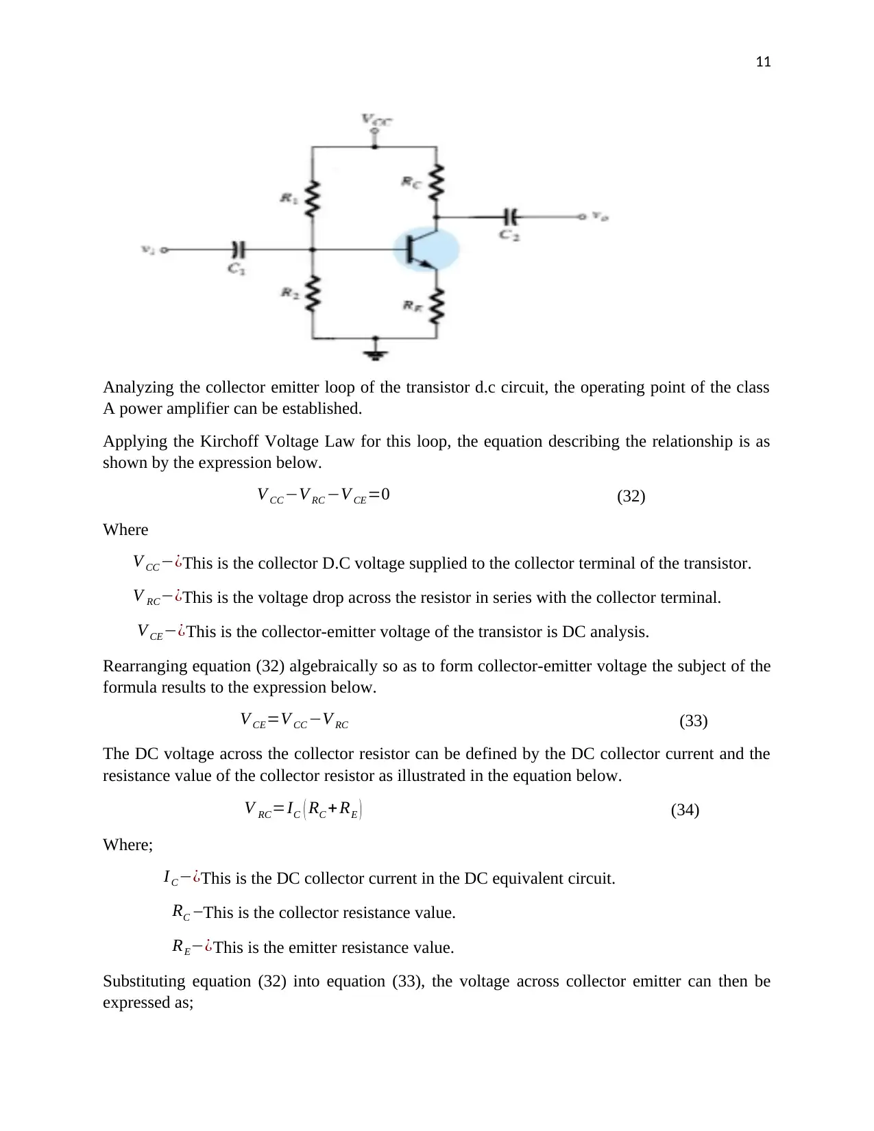
Analyzing the collector emitter loop of the transistor d.c circuit, the operating point of the class
A power amplifier can be established.
Applying the Kirchoff Voltage Law for this loop, the equation describing the relationship is as
shown by the expression below.
V CC −V RC −V CE=0 (32)
Where
V CC −¿This is the collector D.C voltage supplied to the collector terminal of the transistor.
V RC−¿This is the voltage drop across the resistor in series with the collector terminal.
V CE−¿This is the collector-emitter voltage of the transistor is DC analysis.
Rearranging equation (32) algebraically so as to form collector-emitter voltage the subject of the
formula results to the expression below.
V CE=V CC −V RC (33)
The DC voltage across the collector resistor can be defined by the DC collector current and the
resistance value of the collector resistor as illustrated in the equation below.
V RC=IC ( RC + RE ) (34)
Where;
I C−¿This is the DC collector current in the DC equivalent circuit.
RC –This is the collector resistance value.
RE−¿This is the emitter resistance value.
Substituting equation (32) into equation (33), the voltage across collector emitter can then be
expressed as;
12
V CE=V CC −IC ( RC + RE ) (35)
When the transistor is operating as power amplifier, then the desired region of operation should
be characterized by linear relationship between base current and collector current of the
transistor. Therefore, the transistor in a power amplifier configuration should operate in the
active region, which results to the desired amplification of the input base signals. In the active
region, the base current and collector current is related as in the expression below.
I C=β IB (36)
Where;
IB−¿This is DC base current in the DC equivalent circuit
β−¿This is the current gain of transistor.
By substituting equation (34) into equation (33), therefore, the collector-emitter voltage is
denoted as;
V CE=V CC −β IB ( RC + RE ) (37)
From equation (33) and (35), it can be concluded that as base current increases, collector current
increases accordingly. The overall effect leads to reduction of voltage across collector and
emitter. In this design, following parameters in table (4) were used.
Table 4;
V CC 12 V
β=hfe 370
RC 74.33 Ω
RE 0.5 kΩ
N/B β is the current gain retrieved from BC109 datasheet.
Substituting the values in equations (33) and (35)
V CE=12 V −I C ( RC + RE )
V CE=12V −β I B ( RC +RE ) } (38)
In the cut-off region, provided by the condition of insufficient biasing base voltage;
The base current is zero. Mathematically, the expressions are;
V B <V BE=0.7 V } Insufficient biasing (37)
⊘ This is a preview!⊘
Do you want full access?
Subscribe today to unlock all pages.
Trusted by 1+ million students worldwide
1 out of 27
Related Documents


Your All-in-One AI-Powered Toolkit for Academic Success.
+13062052269
info@desklib.com
Available 24*7 on WhatsApp / Email
![[object Object]](/_next/static/media/star-bottom.7253800d.svg)
Unlock your academic potential
Copyright © 2020–2026 A2Z Services. All Rights Reserved. Developed and managed by ZUCOL.