ELEC6251 Assignment 2: Design and Simulation of Power Converters

Verified

Added on  2022/11/09

|12
|1636
|141
Homework Assignment
AI Summary
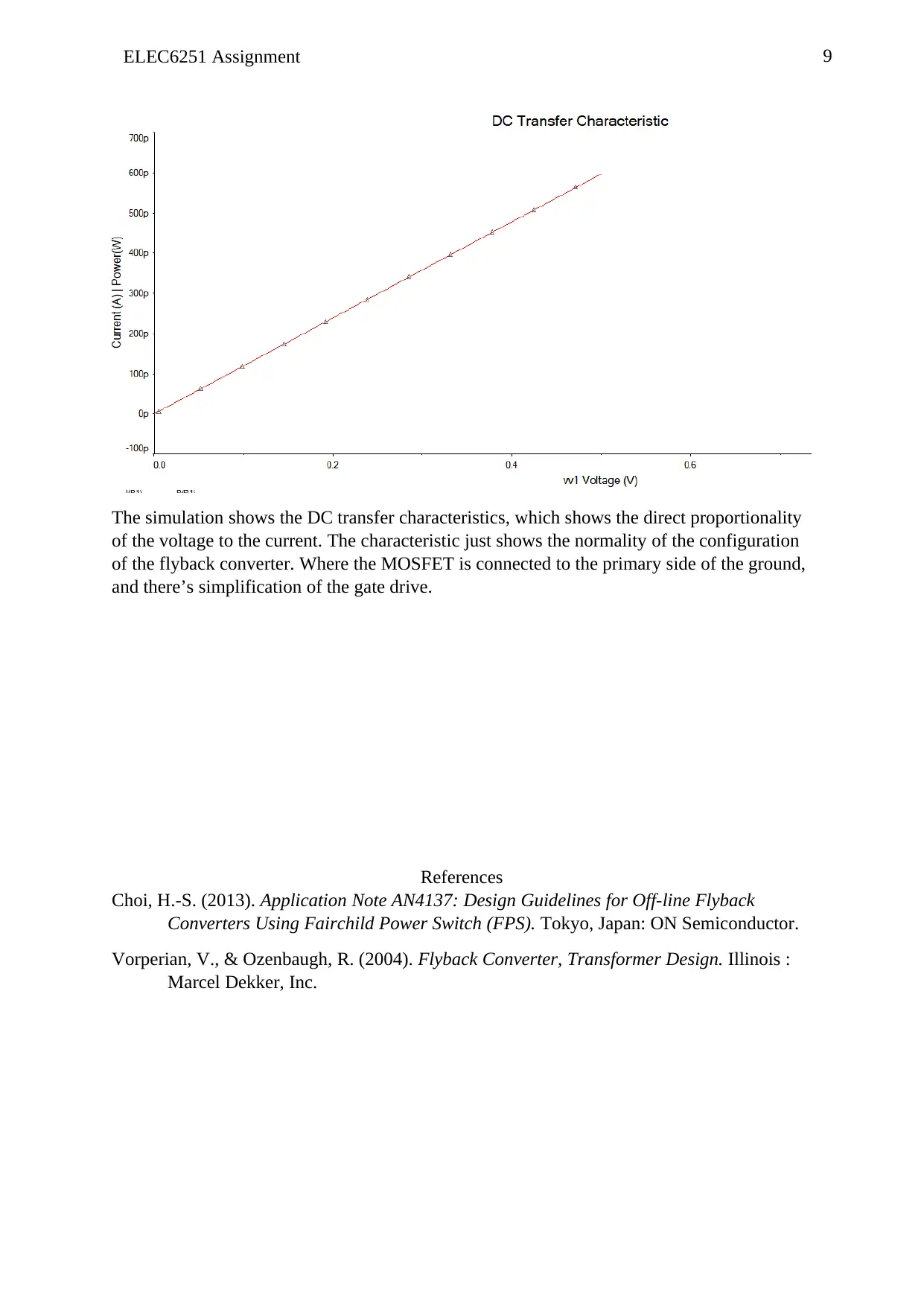
This document presents a comprehensive solution to ELEC6251 Assignment 2, focusing on the design, analysis, and simulation of forward and flyback converters. The assignment involves detailed calculations and component selection to achieve specified output voltages and ripple characteristics. For the forward converter, the solution explores the impact of component values, switching frequency, and duty cycle on performance, including transformer reset methods and ripple factor calculations. The flyback converter section covers similar design considerations, including the determination of switching frequency, MOSFET current, and wire diameters for windings. The solution also includes detailed equations, simulation results, and references to relevant literature, offering a complete understanding of power converter design principles and practical application. The analysis covers key parameters such as input voltage, output voltage, output power, and ripple factors, providing a comprehensive understanding of the converters' behavior under various operating conditions. The document also explains the DC transfer characteristics and the normality of the flyback converter configuration, providing a complete overview of the design and its operation.
Document Page
1Running head: ELEC6251 Assignment
ELEC6251 Assignment
[Name]
[Institutional affiliation]
tabler-icon-diamond-filled.svg

Paraphrase This Document

Need a fresh take? Get an instant paraphrase of this document with our AI Paraphraser
Document Page
2ELEC6251 Assignment
Forward converter
To get the desired output and ripple voltage to be 5V and 25mV respectively, the resistor had
to be increased 50k and the inductor 10mH, and the capacitor ratings of 10u. When the
MOSFET with the specified, the components changed to 2M R1, 1pF C1, and 50mH for L1.
The switching frequency is determined by closing the switch, and the choice is based on the
compromise that the quality that the power supply has with respect to the load and the
switching losses that is fed into the components (often has a direct proportionality to the
switching frequency).
The timing resistor gives a constant off-time of 6μs, and we have chosen around 80% duty
cycle, the on-time duty cycle gave 20μs, therefore the switching frequency came to 40kHz.
The change of value was discovered to be the supply voltage and the timing resistor, it was
changed. These parameters changed the duty cycle of the MOSFET we had in the circuit.
In calculations are shown below:
Document Page
3ELEC6251 Assignment
Specification of input power
We must consider the line frequency (fL):
Parameters to be considered, estimated frequency (Eff) and max power output (Po)
Eff can be set to be a range of 0.7 to 0.75, when the voltage is low, and when the voltage is
high the range is 0.8 to 0.85. the MOSFET has a voltage stress that is twice the voltage input
P¿= Po
Eff
. (1)
Determine the reset method for the transformer and the max. duty ratio
One original limitation that the forward converter has is that there must be a reset of the
transformer when the MOSFET is at off state. This determination can be made by first,
getting the auxiliary winding reset, which the circuit diagram has, the schematic has some
advantages in terms of frequency, because the stored energy in the inductor goes to the input.
V ds
max=V DC (1+ N p
Nr ) (2 )
Dmax N p
N p + N r
. (3)
Where Nr and Np are the turns number for the reset and primary winding respectively. In
equation (2) and (3), the maximum voltage shown on MOSFET is reduced by reducing the
value of Dmax. But when Dmax results are reduced where on the secondary side voltage stress is
increased, means that Nr and NP are equal, therefore we would set Dmax to 0.45. From that we
can determine the secondary and primary turns, reset turns, and turns ratio.
The Ripple factor of the inductor current is obtained by:
K RF= l
2 lO
(4)
Where, lO is the maximum current output, when we do simulation, we get IO to be 2.5μA, the
l is the gradient of the current and voltage curve. Ripple factor shall be obtained and will
aid in the attainment of the peak current and the rms value of the MOSFET,
I ds
peak =IEDC ( 1+K RF ) .. ( 5 )
I ds
rms=IEDC ( 3+K RF
2
) Dmax
3 ..(6)
Were;
I EDC= P¿
V DC
min Dmax
.. ( 7 )
Document Page
4ELEC6251 Assignment
Transformer windings
The first step to this is to obtain the turns ratio, to be the reference point.
n= N p
N sl
= V DC
min Dmax
V o 1+V F 1
. ( 8 )
Where, Ns1 and NP are the turns number of the reference output and the primary side
respectively. V F 1 is the forward voltage drop of the diode, andV o 1 is the output voltage of the
point of reference.
After which, we obtain the integer numbers appropriate for Nsl for the value of N p achieved
be larger than N pmin which is gotten from (9) below:
N p
min= V DC
min Dmax
Ae f s B × 106 (turns) (9)
The magnetizing inductance on the transformer’s primary side is obtained as follows:
Lm= AL × N p
2 × 10⁹ ( H ) .. .(10)
Where, AL is the value of AL without a gap measured in nH/tunrs2
The nth output turns are therefore obtained by
Ns ( n ) = V o ( n ) +V F ( n )
V o 1 +V F 1
N s 1 ( turns ) . ( 11 )
Where, Vo(n) is the voltage output and VF(n) is the diode forward voltage drop that the nth
output has. These can be obtained from the simulation and the other previous calculation.
tabler-icon-diamond-filled.svg

Paraphrase This Document

Need a fresh take? Get an instant paraphrase of this document with our AI Paraphraser
Document Page
5ELEC6251 Assignment
From the current voltage curve, we can see that the current remains zero, meaning the circuit
is non operative for sometime. this happens such that at certain voltage it’s when the current
rises steadily until it reaches a maximum point. Initially there’s a drive that is applied to the
MOSFET, Q1, the current at the secondary shall flow through the capacitor and the inductor,
then to the load. This happens because of the action of the transformer. There will be a
magnetizing current that will build up in the transformer primary meanwhile. The base drive
at Q1 is turned off, and so is the magnetizing current building at the primary. This
magnetizing current begins to flow through the demagnetizing winding, and so the rise of the
current shown in the curve. It will get to a point after a moment and it will switch off.
When there’s no inductor resistance, meaning the inductance is 0H, meaning we have the
capacitance and the resistance from the load. The magnetizing current is in parallel with the
primary winding, so when current is added the current flows through the primary switch.
The value of rms of the current that flows through the MOSFET under the stated scenarios,
assuming that the Is.mean and Is, which are the mean current of the primary added to a half of
the peal-peak magnetizing ripple current, and primary current ripple added to a half of peak
to peak magnetizing ripple current, their values being 1.6, and 0.24 respectively.
I S , max , RMS=IS mean D 1+ 1
3 ( is
I S . mean )2
=4.5 Arms
Where D = 50%
The three diodes: When the inductance is zero, D1 will recover slowly, and there will be a
significant amount of current. There will be a maximum duty cycle, that means D = 0.5,
remember the voltage input V1= 12
I DI , max, RMS= V imax
LM
1
Dmax
fs
3 =0 .6 5 Arms
Document Page
6ELEC6251 Assignment
The duty cycle that has been considered is 50%, this gives us a maximum voltage.
When getting the load resistance, we first find the capacitance Co(n), which shall be 200μF
(that will give the required output voltage)
V o (n ) = Io (n ) KRF
4 CO ( n ) f s
+2 K RF IO ( n ) Rc ( n ) . ( 12 )
Where,
Co (n )Rc(n) is the capacitance and effective series resistance respectively. We shall set the
K RF, current ripple factor to 0.2, f s, shall be 40kHz, the current is 2.5μA. when substituted,
the value shall be 80KΩ,
Flyback converter
An output voltage is achieved by the capacitor being 300nF and the load resistor having a
reading of 800MΩ. The input DC voltage is equal to the output voltage, 12V.
In the calculations, we shall consider the following parameters:
Input voltage 12VDC
Output voltage VO=12 V
Document Page
7ELEC6251 Assignment
Output power PO = 0.5Watt
Output voltage ripple δVO = 200mV
Switching frequency f s 200 kHz
On the theoretical design of a flyback converter, the parameters we would like to look at are:
The switching frequency
The magnitude is given by 23.8dB
Frequency can be obtained from this by saying change 23.8dB to frequency, by calculating
and using 1Hz as the reference point, we have 142kHz.
We shall set the Dmax to be 0.5, KRF to be 0.5, since for a flyback converter it should be set
from 0.25-0.5.
The inductance on the primary side of the transformer
Lm= (V DC
Min Dmax )2
2 P¿ f s K RF
.(13)
Lm= ( 12 ×0.5 ) 2
1 ×142× 106 ×0.5 =0.51 mH
The MOSFET RMS current and the maximum peak current, during the normal operation can
also be obtained by:
I ds
Peak=I EDC + I
2 (14)
and,
I ds
rms= [3 ( IEDC )2 + ( I
2 )2
] Dmax
3 .(15)
Where,
IEDC= P¿
V DC
min Dmax
(P¿=0.625 W , having Eff =0.8) (16)
And
I = V DC
min Dmax
Lm f s
..(17)
Substituting, we have: (17) = 9.804A, (16) =0.25A; (15) = 1.887A, and (14) =4.852A
tabler-icon-diamond-filled.svg

Paraphrase This Document

Need a fresh take? Get an instant paraphrase of this document with our AI Paraphraser
Document Page
8ELEC6251 Assignment
Determine the diameter of the wire for each winding, by obtaining the rms current of
each output
To get this we have to first find the load occupying factor K L(n ), which is given by:
K L ( n ) = PO ( n )
Po
( 1 8 )
Which in our case is 1, since the max power output (PO(n) and power output are the same.
We also need to establish the value of VRO, which is the reflected output voltage in the
primary, these are imposed in the MOSFET
V RO= Dmax
1Dmax
V DC
min .. ( 1 9 )
Therefore, the value of VRO is 12V too.
I sec (n)
rms =I ds
rms
1Dmax
Dmax
V RO K L
V O (n )+ V F (n)
.(20)
Where, V F (n ) is the diode forward voltage drop, which is 12mV. Therefore, I sec (n)
rms =1.885A
The output capacitor
Here we shall consider the ripple current and voltage, where the ripple current is obtained by,
this goes through the capacitor (CO(n))
ICap ( n )
rms = ( ID ( n )
rms
) 2
IO ( n )
2 . ( 21 )
But I D ( n )
rms = I sec (n)
rms , and IO is the load current, (which is obtained through the power,
0.04167A), the answer becomes 1.885A
To find the capacitance and the resistor (load resistance), we shall use the following equation
V o(n)= Io(n) Dmax
CO (n) f s
+ I ds
peak V RO RC(n) KL(n)
V O (n)+V F (n)
(22)
0.012= 6.5
CO(n)
+4.85 RC (n) ..(23)
Equation (23) finds us the capacitance in terms of the resistance, it defines the relationship of
the two variables in the circuit.
Document Page
9ELEC6251 Assignment
The simulation shows the DC transfer characteristics, which shows the direct proportionality
of the voltage to the current. The characteristic just shows the normality of the configuration
of the flyback converter. Where the MOSFET is connected to the primary side of the ground,
and there’s simplification of the gate drive.
References
Choi, H.-S. (2013). Application Note AN4137: Design Guidelines for Off-line Flyback
Converters Using Fairchild Power Switch (FPS). Tokyo, Japan: ON Semiconductor.
Vorperian, V., & Ozenbaugh, R. (2004). Flyback Converter, Transformer Design. Illinois :
Marcel Dekker, Inc.
Document Page
10ELEC6251 Assignment
Appendix
tabler-icon-diamond-filled.svg

Paraphrase This Document

Need a fresh take? Get an instant paraphrase of this document with our AI Paraphraser
Document Page
11ELEC6251 Assignment
Document Page
12ELEC6251 Assignment
chevron_up_icon
1 out of 12
circle_padding
hide_on_mobile
zoom_out_icon
[object Object]