Power Electronics Homework: Boost Converter Analysis and Design

Verified

Added on  2022/08/24

|5
|505
|17
Homework Assignment
AI Summary
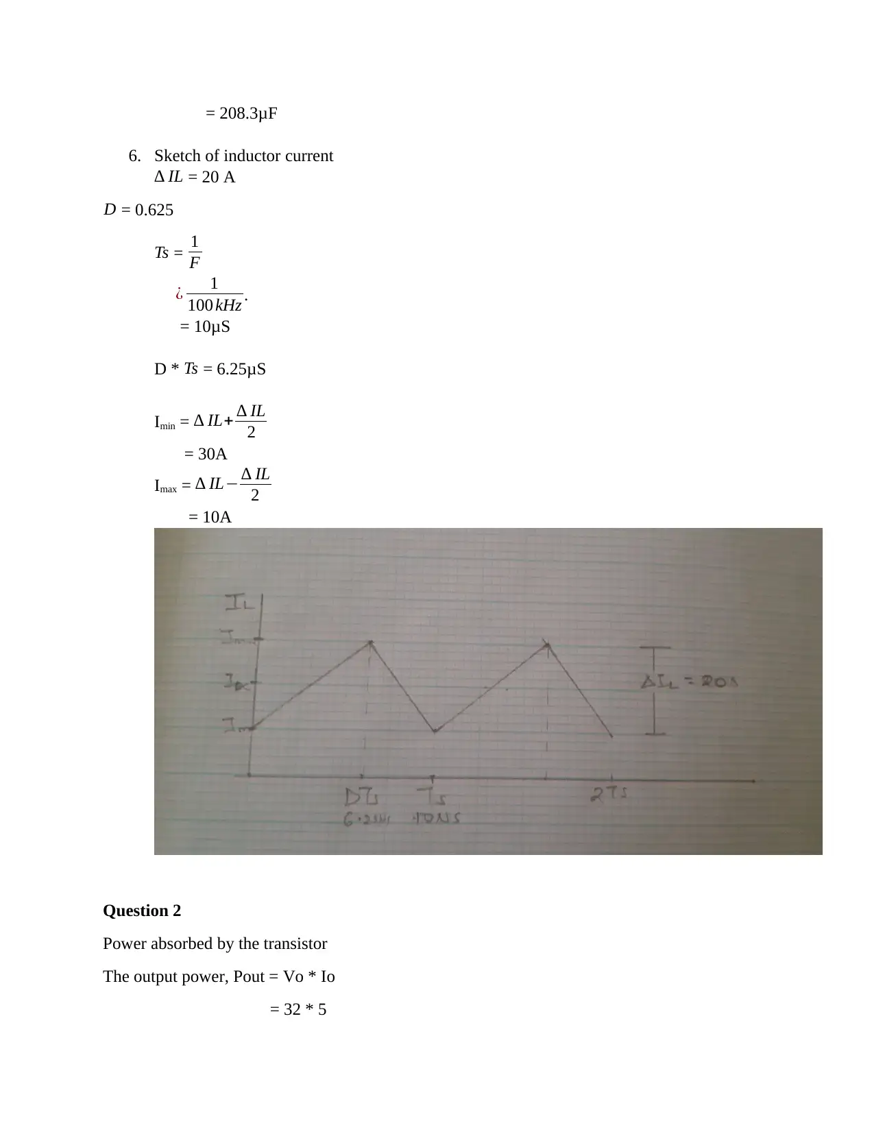
This document presents a comprehensive solution to a power electronics assignment. The solution covers the analysis and design of a boost converter circuit, including calculations for the duty cycle, inductor, and capacitor values. It also includes analysis of power dissipation in the circuit components such as the transistor, inductor, and diode. The document provides a step-by-step approach to solving the problems, along with relevant formulas and equations. It also includes references to power electronics handbooks. This assignment is a valuable resource for students studying power electronics, providing a clear understanding of boost converter operation and design.
Document Page
Question 1
1. The circuit represent boost converter.
2. Value of load resistor, RL is computed as shown below
From ohm’s law relationship
V = R * I
Therefore, RL = Vout
Io
= 32
5
= 6.4Ω
3. Duty cycle is computed using the following relationship
Vo
Vs = 1
1D
Where Vo is the output and Vs is the input of the converter
Making D the subject of the formula
D = V oVs
Vo
= (32 – 12) / 32
= 0.625
4. Minimum value of an inductor
The relationship between inductance and ripple current is given by the equation below
L = VsD
IlF
Substituting the values of the equation above we get
= 120.625
20100103
= 3.75 μH
5. Capacitor value
Minimum capacitance value that will give a ripple voltage of 150mV is given by the
equation below
C.min = DVo
VppFR [1]
= 0.62532
1501031001036.4
tabler-icon-diamond-filled.svg

Paraphrase This Document

Need a fresh take? Get an instant paraphrase of this document with our AI Paraphraser
Document Page
= 208.3μF
6. Sketch of inductor current
IL = 20 A
D = 0.625
Ts = 1
F
¿ 1
100 kHz .
= 10μS
D * Ts = 6.25μS
Imin = IL+ IL
2
= 30A
Imax = IL IL
2
= 10A
Question 2
Power absorbed by the transistor
The output power, Pout = Vo * Io
= 32 * 5
Document Page
= 160 W
IL = Pout / Vs
= 160 / 12
= 13.33A
Power absorbed by the transistor, Pt = IL2 * RDS
= 13.332 * 0.1
= 17.78W
Power absorbed by the inductor, Pi = IL2 * Rparasitic
= 13.332 * 0.1
= 17.78W
Power absorbed by the diode, Pd = ID * Vd
ID = Io * D = 5 * 0.625 = 3.125
Pd = ID * Vd
= 3.125 * 0.4
= 1.25 W
Input power, Pin = IL * Vs
= 13.33 * 12
= 160W
Output power, Pout = Pin – PLosses
= 160 – (17.78 + 17.78 + 1.25)
= 123.19W
The output voltage, Vout = Pout / Io
= 123.19 / 5
= 24.63 V
Question 3
Input voltage, Vin = 5V
Document Page
Output voltage, Vout = 1.33V
Switching frequency, F = 100kHz
Duty cycle, D of q+ = t . on
t . on+t .0 ff = Vout
Vin
= 1.33
5
= 0.266
Duty cycle, D of q- = 1 – 0.266 = 0.734
Normally, the duty cycle of q+ is used for computation of the entire circuit.
The equation relating the inductor ripple current and the inductor is given by the equation below
Lmin = ( VinVout )D
F Il ,
where Vin is the input voltage, Vout the output voltage, D is the duty cycle, F is the switching
frequency and Il is inductor ripple current.
Substituting the values of the equation above
Lmin = ( 51.33 )0.266
100 kHz100 mA ,
= 97.622μH.
The equation relating the capacitor ripple voltage and the capacitance is given by the equation
below
Cmin = Il
8 VppF [2]
= 100103
820103100103
= 6.25F.
tabler-icon-diamond-filled.svg

Paraphrase This Document

Need a fresh take? Get an instant paraphrase of this document with our AI Paraphraser
Document Page
REFERENCES
[1] M, Rashid,Ed, Power electronics handbook. London: Butterworth-Heinemann, 2017.
[2] A, Emadi,A, Khaligh, Z,Nie and Y, Lee. Integrated power electronic converters and
digital control. Florida: CRC Press,2017.
chevron_up_icon
1 out of 5
circle_padding
hide_on_mobile
zoom_out_icon
[object Object]