Capstone Project: Automated Power Factor Correction with PLC System
VerifiedAdded on 2022/10/04
|25
|4135
|46
Report
AI Summary
This report details a capstone project focused on automated power factor correction using Programmable Logic Controllers (PLCs). The project addresses the problem of reduced power factor in AC power systems due to inductive loads. The report outlines the methodology, including the use of an interfacing circuit with current and phase angle detectors, and the implementation of a PLC to control capacitor banks. The objectives are to automatically correct the power factor, maintaining it at 0.9 or greater. The report covers the design of the hardware components, including the PLC module, switching circuits with relays and triacs, and the calculations for power factor correction. It also includes software implementation details, such as ladder diagrams and flowcharts for PLC control. The project aims to improve power system efficiency by automatically adjusting the power factor through the addition or removal of capacitors based on the load requirements. The report concludes with a discussion of the project's outcomes, including the development of an operating prototype and a detailed drawing package, along with the presentation of the design choices and calculations.

ELECTRICAL POWER
Name of Student
Institution Affiliation
Name of Student
Institution Affiliation
Paraphrase This Document
Need a fresh take? Get an instant paraphrase of this document with our AI Paraphraser
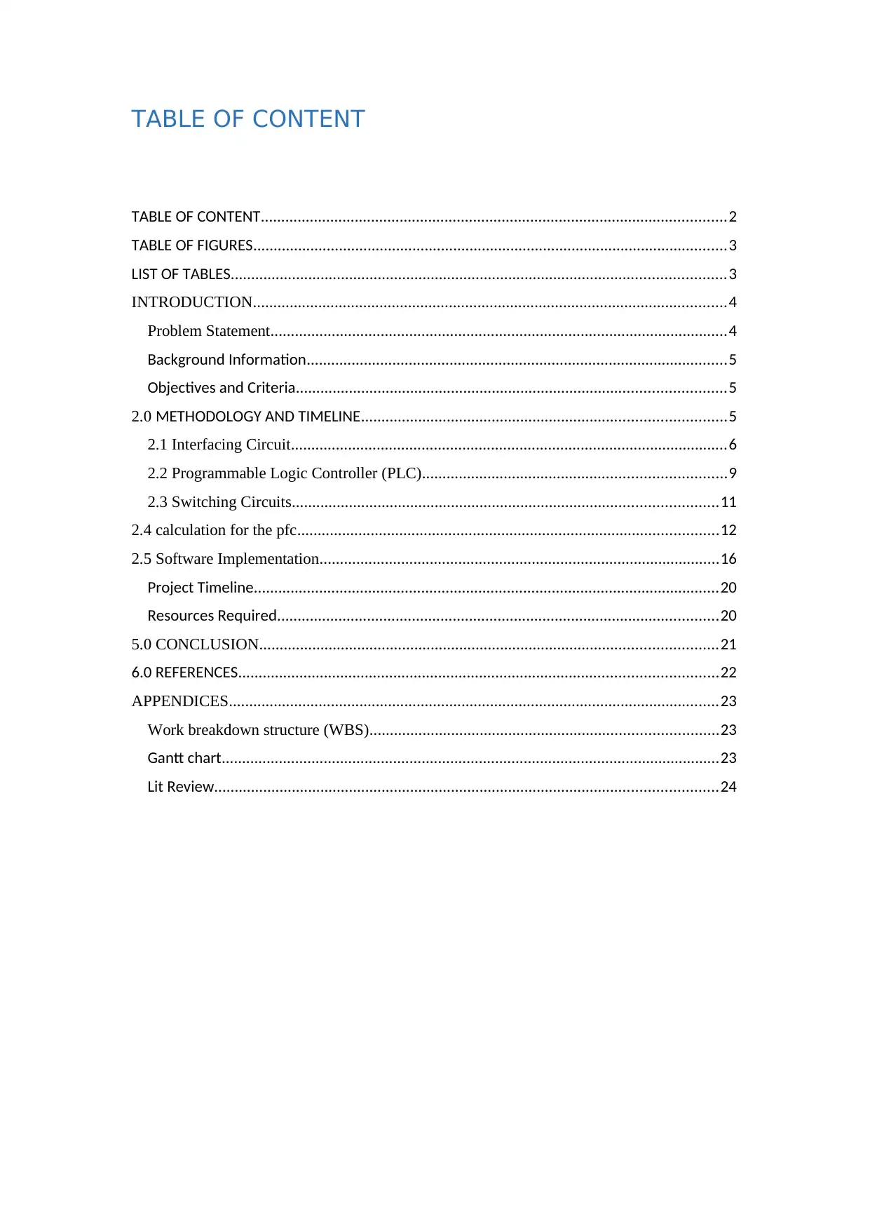
TABLE OF CONTENT
TABLE OF CONTENT..................................................................................................................2
TABLE OF FIGURES....................................................................................................................3
LIST OF TABLES.........................................................................................................................3
INTRODUCTION....................................................................................................................4
Problem Statement................................................................................................................4
Background Information.......................................................................................................5
Objectives and Criteria.........................................................................................................5
2.0 METHODOLOGY AND TIMELINE.........................................................................................5
2.1 Interfacing Circuit...........................................................................................................6
2.2 Programmable Logic Controller (PLC)..........................................................................9
2.3 Switching Circuits........................................................................................................11
2.4 calculation for the pfc.......................................................................................................12
2.5 Software Implementation..................................................................................................16
Project Timeline..................................................................................................................20
Resources Required............................................................................................................20
5.0 CONCLUSION................................................................................................................21
6.0 REFERENCES.....................................................................................................................22
APPENDICES........................................................................................................................23
Work breakdown structure (WBS).....................................................................................23
Gantt chart..........................................................................................................................23
Lit Review...........................................................................................................................24
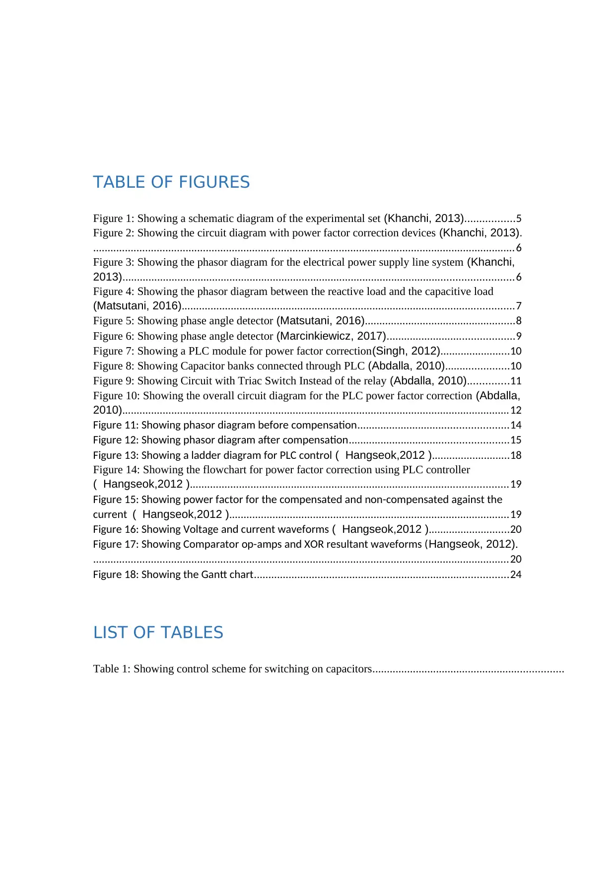
TABLE OF FIGURES
Figure 1: Showing a schematic diagram of the experimental set (Khanchi, 2013).................5
Figure 2: Showing the circuit diagram with power factor correction devices (Khanchi, 2013).
..................................................................................................................................................6
Figure 3: Showing the phasor diagram for the electrical power supply line system (Khanchi,
2013).......................................................................................................................................6
Figure 4: Showing the phasor diagram between the reactive load and the capacitive load
(Matsutani, 2016)...................................................................................................................7
Figure 5: Showing phase angle detector (Matsutani, 2016)....................................................8
Figure 6: Showing phase angle detector (Marcinkiewicz, 2017)............................................9
Figure 7: Showing a PLC module for power factor correction(Singh, 2012)........................10
Figure 8: Showing Capacitor banks connected through PLC (Abdalla, 2010)......................10
Figure 9: Showing Circuit with Triac Switch Instead of the relay (Abdalla, 2010)..............11
Figure 10: Showing the overall circuit diagram for the PLC power factor correction (Abdalla,
2010)......................................................................................................................................12
Figure 11: Showing phasor diagram before compensation....................................................14
Figure 12: Showing phasor diagram after compensation.......................................................15
Figure 13: Showing a ladder diagram for PLC control ( Hangseok,2012 )...........................18
Figure 14: Showing the flowchart for power factor correction using PLC controller
( Hangseok,2012 )..............................................................................................................19
Figure 15: Showing power factor for the compensated and non-compensated against the
current ( Hangseok,2012 ).................................................................................................19
Figure 16: Showing Voltage and current waveforms ( Hangseok,2012 )............................20
Figure 17: Showing Comparator op-amps and XOR resultant waveforms (Hangseok, 2012).
................................................................................................................................................20
Figure 18: Showing the Gantt chart........................................................................................24
LIST OF TABLES
Table 1: Showing control scheme for switching on capacitors..................................................................
⊘ This is a preview!⊘
Do you want full access?
Subscribe today to unlock all pages.
Trusted by 1+ million students worldwide

INTRODUCTION
Due to the presence of several inductive loads along with the power system
like the transformers and inductive motors the value of the reactance will highly
increase. When the reactance is higher than reactive power will be higher which result
in unwanted power loss in the power line. Therefore this need to look for a way of
reducing the higher reactive power. When the reactive power is higher it means that
the power factor is lower. So boosting of the power factor will reduce the reactance
which will hence reduce the reactive power. This can be done by adding the
capacitors to the power line system. The addition of the capacitance can now be added
automatically depending on the required through the use of programmable logic
controllers.
Problem Statement
When AC power is transmitted, the induction in the system causes a reduction
of the power factor. Adding an inductive load further affects the power factor. For this
reason, capacitors can be used to compensate for the effect of them in the power line
system. This project will use automated PLCs to add or remove capacitors to maintain
or adjust the power factor in the power line system and to stabilize the efficiency.
Background Information
PLC is a computer-based software which is employed in controlling several
automated tasks. The use of PLC makes work easier as there is no need for human
intervention in controlling the system like the addition of capacitor bank into the
power line to adjust the power factor to the required level. The PLC system is a
smaller device and more efficient to use as compared to human being which can make
Paraphrase This Document
Need a fresh take? Get an instant paraphrase of this document with our AI Paraphraser

some mistakes due to the calculation of the required amount of capacitor required for
the correction. This paper hence addresses power factor correction in the power line
system with the induction motor as the reference point. The cause of the lower power
factor in the power line system is the nature of the load which is the inductive load.
Objectives and Criteria
The objective of this project is to automatically correct the power factor
through the use of programmable logic controllers. This concept is made possible
through the addition of capacitors which are connected into the power supply circuit.
The controller will connect the required amount of capacitance according to the power
factor required in the system.
2.0 METHODOLOGY AND TIMELINE
The hardware of this includes the three-phase supply, PLC, capacitor bank for 3
phase, interfacing circuit. These can be illustrated schematically as below;
Figure 1: Showing a schematic diagram of the experimental set (Khanchi, 2013).
2.1 Interfacing Circuit
The interfacing circuit consists of 2 key components which are the current peak
detector and the phase angle detector (Arya, 2012). Most supply system must have
capacitor banks to reduce the reactance and reactive power, the circuit can hence be
summarized as below;
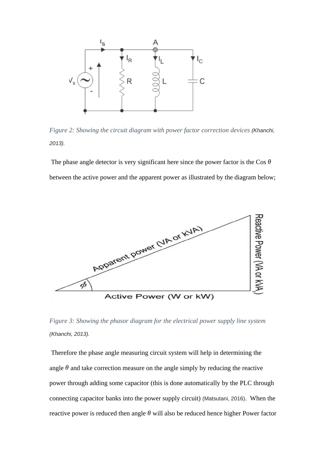
Figure 2: Showing the circuit diagram with power factor correction devices (Khanchi,
2013).
The phase angle detector is very significant here since the power factor is the Cos θ
between the active power and the apparent power as illustrated by the diagram below;
Figure 3: Showing the phasor diagram for the electrical power supply line system
(Khanchi, 2013).
Therefore the phase angle measuring circuit system will help in determining the
angle θ and take correction measure on the angle simply by reducing the reactive
power through adding some capacitor (this is done automatically by the PLC through
connecting capacitor banks into the power supply circuit) (Matsutani, 2016). When the
reactive power is reduced then angle θ will also be reduced hence higher Power factor
⊘ This is a preview!⊘
Do you want full access?
Subscribe today to unlock all pages.
Trusted by 1+ million students worldwide

/ Cosθ. The automatic connection of the capacitor into the power line system help in
the reduction of the reactive power as illustrated in equation 1 below, and this is also
explained further in the below diagram;
Figure 4: Showing the phasor diagram between the reactive load and the capacitive
load (Matsutani, 2016).
XT= XL-XC . . . . . . . . . . . . . . . . . . . . . . . . . . . . . . . . . . . . . . . . . . . . . . . . . . . . . . . . . . 1
And the reactive power is obtained using the below equation 2;
Q= IX2XT . . . . . . . . . . . . . . . . . . . . . . . . . . . . . . . . . . . . . . . . . . . . . . . . . . . . . . . . . . 2
Where Q is the reactive power, XT is the resultant reactance of the system in ohms, IX
is the reactance current.
The phase angle detector is hence illustrated using the following diagram;
Paraphrase This Document
Need a fresh take? Get an instant paraphrase of this document with our AI Paraphraser
Figure 5: Showing phase angle detector (Matsutani, 2016).
Phase angle measuring unit which is shown in figure five above comprises of the
comparison stage, converting stage, XOR stage and the clipping stage (Deaver, 2010).
For the first stage in the above diagram, the input sinusoidal current is changed to the
square waveform. Through the use of the comparator op-amp. In the same way, the
measured voltage which is in the sinusoidal waveform is converted into a square
waveform. The voltage and the current square waveforms are then compared logic
comparison of the XOR is done (Gumaer, 2017). At the final stage through taking the
stage 2 output. All the negative present peak waveform are clipped at this stage. The
results from the port six as shown in figure six below is fed up to non-inverting
terminals of the peak detector circuit. The output is then conditioned to be a square
waveform (Marcinkiewicz, 2017). This square wave amplitude is trapped in capacitor
banks which then results in a signal. The resultant signal is then fed to the PLC analog
input port. The signal detected is then scaled appropriately so as to obtain the required
results.

Figure 6: Showing phase angle detector (Marcinkiewicz, 2017).
2.2 Programmable Logic Controller (PLC)
The correction of the power factor is always driven by S7-300 PLC which is
illustrated using figure 7, this model has several models like CPU, digital input, power
supply, digital output and also the ADC ( Analogue-digital converter). The digital
input module has the following specifications; 24 VDC for which for the logic “0” the
voltages ranges from -3 to 5 VDC while for the logic “1” which ranges from 13 to 30
VDC. There is also an analog module which is a 2 channel and also a 12 bit ADC
(Analog to digital converter). The digital output of the PLC has 24VDC and a current
of 0. 5 VDC.
For the power factor correction, the two output of the interfacing can be fed to
the PLC through the following way; The results of the measured phase angle
measuring unit is fed to the digital input module of the programmable logic controller
(Santo, 2013). Here the output of the peak current detector is fed to the ADC module.
The controller will hence calculate the lagging reactive power of the power line
system and with the obtained results the PLC will take an appropriate decision and
gives a signal to the digital output module (Abdalla, 2010). In the digital output
module there is a switching circuit which is connected to the sequence of capacitors in
⊘ This is a preview!⊘
Do you want full access?
Subscribe today to unlock all pages.
Trusted by 1+ million students worldwide
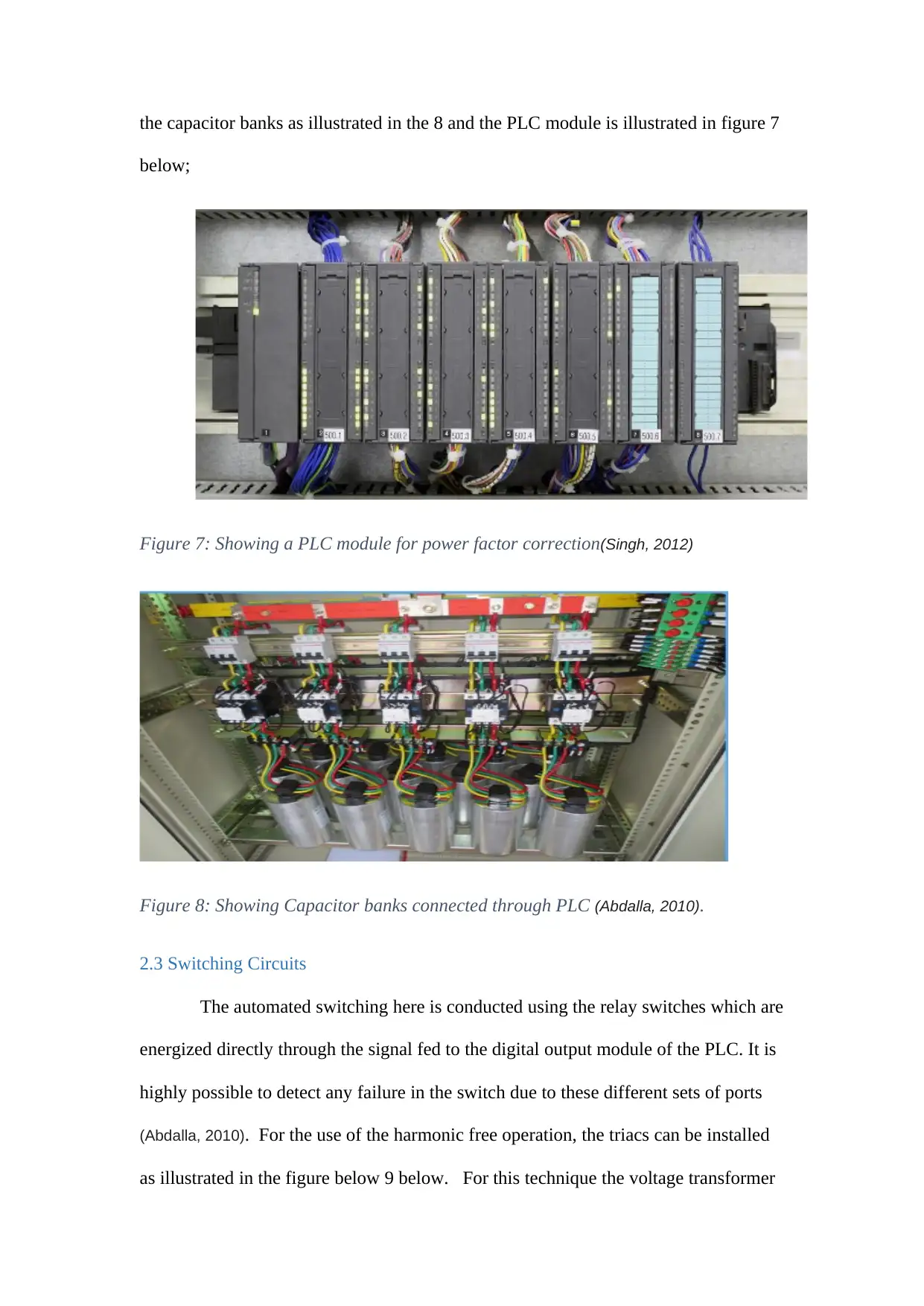
the capacitor banks as illustrated in the 8 and the PLC module is illustrated in figure 7
below;
Figure 7: Showing a PLC module for power factor correction(Singh, 2012)
Figure 8: Showing Capacitor banks connected through PLC (Abdalla, 2010).
2.3 Switching Circuits
The automated switching here is conducted using the relay switches which are
energized directly through the signal fed to the digital output module of the PLC. It is
highly possible to detect any failure in the switch due to these different sets of ports
(Abdalla, 2010). For the use of the harmonic free operation, the triacs can be installed
as illustrated in the figure below 9 below. For this technique the voltage transformer
Paraphrase This Document
Need a fresh take? Get an instant paraphrase of this document with our AI Paraphraser
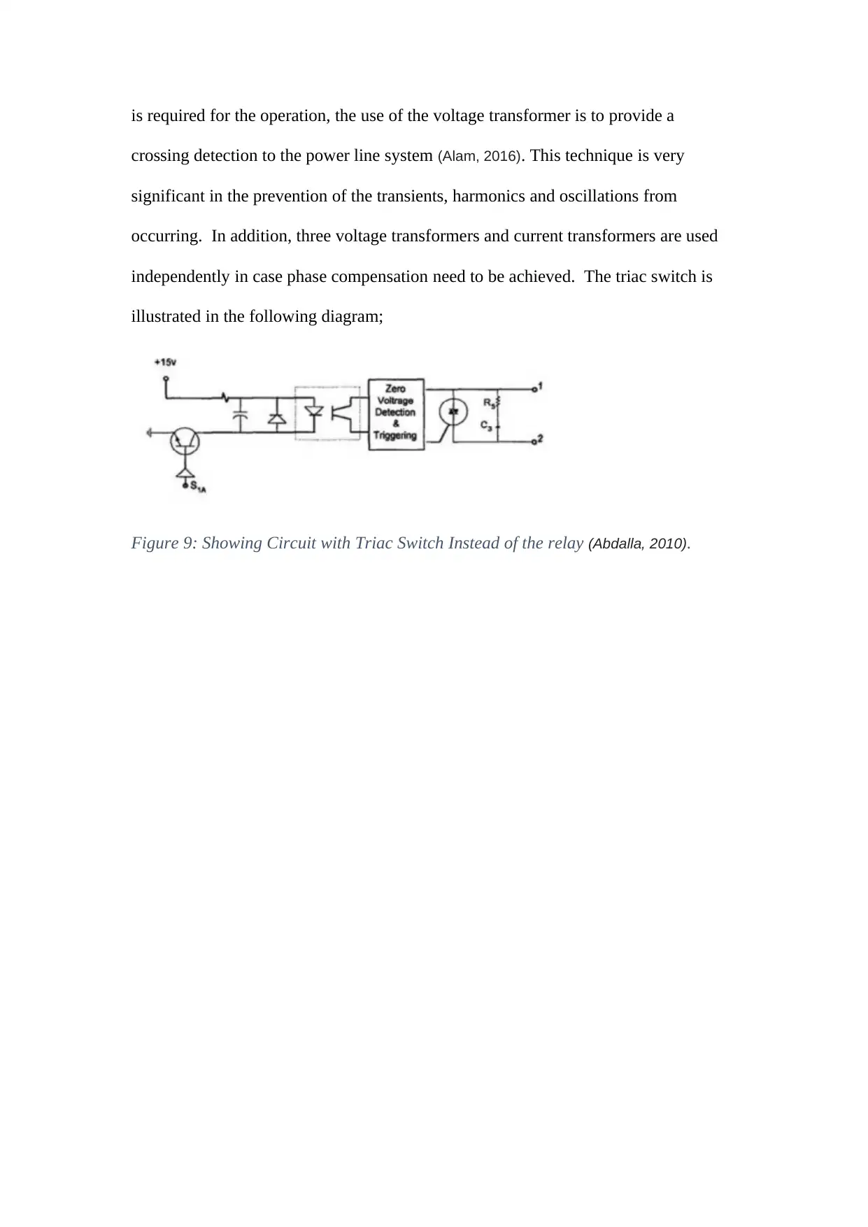
is required for the operation, the use of the voltage transformer is to provide a
crossing detection to the power line system (Alam, 2016). This technique is very
significant in the prevention of the transients, harmonics and oscillations from
occurring. In addition, three voltage transformers and current transformers are used
independently in case phase compensation need to be achieved. The triac switch is
illustrated in the following diagram;
Figure 9: Showing Circuit with Triac Switch Instead of the relay (Abdalla, 2010).
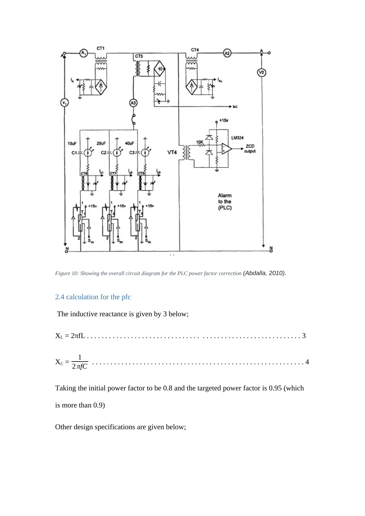
Figure 10: Showing the overall circuit diagram for the PLC power factor correction (Abdalla, 2010).
2.4 calculation for the pfc
The inductive reactance is given by 3 below;
XL = 2πfL . . . . . . . . . . . . . . . . . . . . . . . . . . . . . . . . . . . . . . . . . . . . . . . . . . . . . . . . . . 3
XC = 1
2 πfC . . . . . . . . . . . . . . . . . . . . . . . . . . . . . . . . . . . . . . . . . . . . . . . . . . . . . . . . . . 4
Taking the initial power factor to be 0.8 and the targeted power factor is 0.95 (which
is more than 0.9)
Other design specifications are given below;
⊘ This is a preview!⊘
Do you want full access?
Subscribe today to unlock all pages.
Trusted by 1+ million students worldwide
1 out of 25
Related Documents


Your All-in-One AI-Powered Toolkit for Academic Success.
+13062052269
info@desklib.com
Available 24*7 on WhatsApp / Email
![[object Object]](/_next/static/media/star-bottom.7253800d.svg)
Unlock your academic potential
Copyright © 2020–2026 A2Z Services. All Rights Reserved. Developed and managed by ZUCOL.