BEng Electrical Engineering: Power Supply and Op-Amp Project Report
VerifiedAdded on 2023/06/15
|33
|4467
|355
Report
AI Summary
This report details the design and operation of a power supply unit and various operational amplifier (op-amp) circuits. The power supply design encompasses a stepping down transformer, rectifier, filtering, and voltage regulation. Different types of amplifiers, including inverting, summing, non-inverting, and differential amplifiers, are examined with their specific functions. The report presents experimental results from power supply tests, demonstrating satisfactory performance and insights into signal measurement. The analysis covers the main components of power systems, protections, op-amp circuits, and transformers, providing a comprehensive understanding of their functionality and application. The report includes risk assessment, methodology, results, discussion, and conclusion, supported by relevant diagrams, equations, and a bibliography.

Engineering 1
ENGINEERING
By Name
Course
Instructor
Institution
Location
Date
ENGINEERING
By Name
Course
Instructor
Institution
Location
Date
Paraphrase This Document
Need a fresh take? Get an instant paraphrase of this document with our AI Paraphraser
Engineering 2
ABSTRACT
Electrical energy is the flow of electrons which create electric power. Through the
implementation of the power supply, therefore it is possible to manipulate electrical power at the
output. Power supplies, therefore, are the devices which have the obligation of manipulating the
electrical power to be employed in various applications. A power supply includes input
transformer, rectifier, smoothening and regulator. This report will clearly illustrate the power
supply design and the operation. Amplifier basically is an electronic component which is
employed in the augmentation of the electrical signal. There are several types of amplifiers, some
are; summing, inverting, non- inverting and a differential amplifier. Each type of amplifier
performs a specific function. Power supply unit has been studied with its main components
taking into account protections and op-amp circuits and transformers are also analyzed. When
several experiments are done for the power supply the following results are quite satisfactory and
learned a lot that how to measure the single with respect to the input.
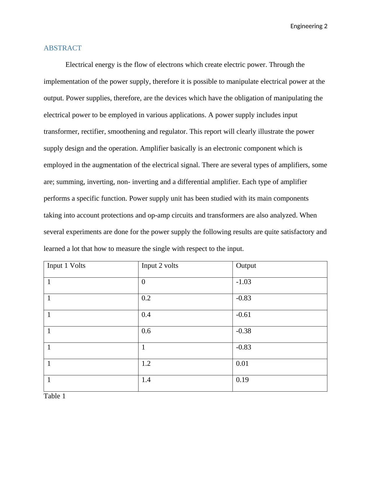
Input 1 Volts Input 2 volts Output
1 0 -1.03
1 0.2 -0.83
1 0.4 -0.61
1 0.6 -0.38
1 1 -0.83
1 1.2 0.01
1 1.4 0.19
Table 1
ABSTRACT
Electrical energy is the flow of electrons which create electric power. Through the
implementation of the power supply, therefore it is possible to manipulate electrical power at the
output. Power supplies, therefore, are the devices which have the obligation of manipulating the
electrical power to be employed in various applications. A power supply includes input
transformer, rectifier, smoothening and regulator. This report will clearly illustrate the power
supply design and the operation. Amplifier basically is an electronic component which is
employed in the augmentation of the electrical signal. There are several types of amplifiers, some
are; summing, inverting, non- inverting and a differential amplifier. Each type of amplifier
performs a specific function. Power supply unit has been studied with its main components
taking into account protections and op-amp circuits and transformers are also analyzed. When
several experiments are done for the power supply the following results are quite satisfactory and
learned a lot that how to measure the single with respect to the input.
Input 1 Volts Input 2 volts Output
1 0 -1.03
1 0.2 -0.83
1 0.4 -0.61
1 0.6 -0.38
1 1 -0.83
1 1.2 0.01
1 1.4 0.19
Table 1
Engineering 3
TABLE OF CONTENT
Contents
ABSTRACT................................................................................................................................................2
INTRODUCTION.......................................................................................................................................3
Purpose of the project..............................................................................................................................5
Aim of the project....................................................................................................................................5
THEORY.....................................................................................................................................................6
Power supply...........................................................................................................................................6
Stepping down transformer..................................................................................................................6
Rectifier...............................................................................................................................................6
Filtering...............................................................................................................................................7
Voltage Regulation..............................................................................................................................8
OP-amp...................................................................................................................................................9
RISK ASSESSMENT...............................................................................................................................15
METHOD..................................................................................................................................................15
Power supply.........................................................................................................................................15
Op-amp..................................................................................................................................................17
1. Inverting amplifier.....................................................................................................................17
2. Summing amplifier....................................................................................................................17
3. Non- Inverting amplifier............................................................................................................17
4. Differential amplifier.................................................................................................................18
RESULTS.................................................................................................................................................18
DISCUSSION...........................................................................................................................................23
CONCLUSION.........................................................................................................................................29
Bibliography...............................................................................................................................................30
Appendix...................................................................................................................................................31
INTRODUCTION
The power that comes from the generation station travels several miles to reach the consumers.
⊘ This is a preview!⊘
Do you want full access?
Subscribe today to unlock all pages.
Trusted by 1+ million students worldwide
Engineering 4
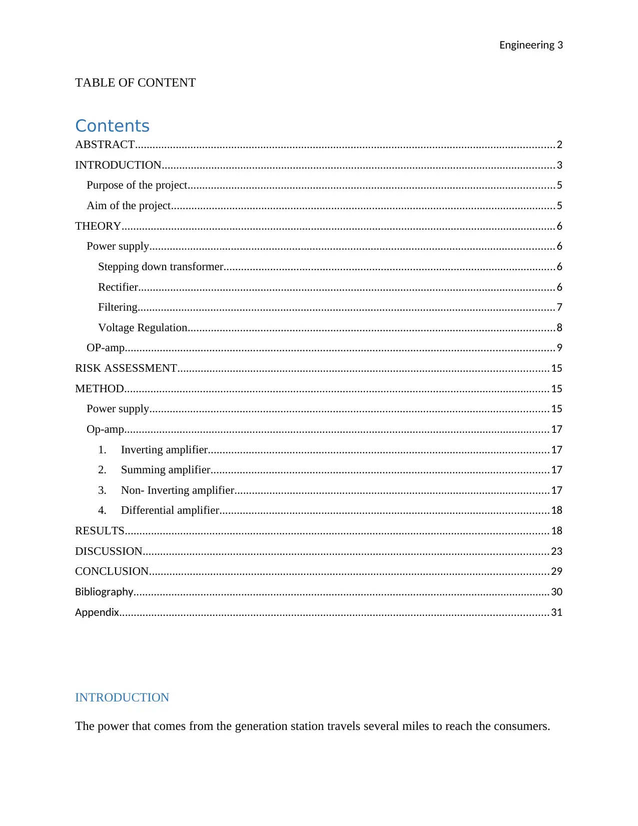
In this case, AC current is employed. AC has different phases depending on the usage of the
power. In disparity to AC, there is DC which doesn't alternate the Current, it has a steady current
at the output to be applied to circuits. DC hence is suitable for circuit design this is due to many
of the components use DC power. Through the wall socket many different devices
Are plugged in and used daily but most of these devices require DC to work correctly.
As the plug is inserted into a socket outlet AC will be converted to DC. This is done using the
full wave rectifier as seen in the diagrams below. The electronics will not use AC but DC.
Fig 1: Showing rectification diagram and waveform after rectification
Operational amplifiers are linear electronic components which can be employed in filtering as
well as doing some mathematical operations such as differentiation, integration, addition and
subtract. OPamp is an electronic device made to be employed with external feedback device like
capacitors and resistors between its output and input terminals. The feedback part governs the
Paraphrase This Document
Need a fresh take? Get an instant paraphrase of this document with our AI Paraphraser
Engineering 5
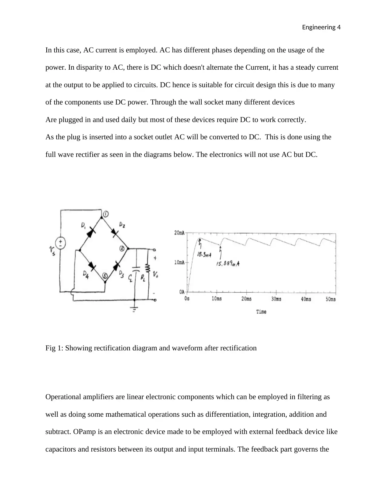
resulting function of the amplifier. The diagram below illustrates the amplifiers for inverting and
non- inverting respectively
Fig 2: Showing the inverting and non-inverting Op-amp with the feedback connected
Purpose of the project
The purpose of this project is to develop a power supply unit having rectifier for voltage
regulation which can be used by electronic appliances. The project will as well help in stepping
down the voltage to smaller values which can be used by low voltage devices like LED.
Aim of the project
The aim of this project is to study and analyze the main components of power systems taking
into account protections and op-amp circuits and transformers (Bird, 2013).
Engineering 6
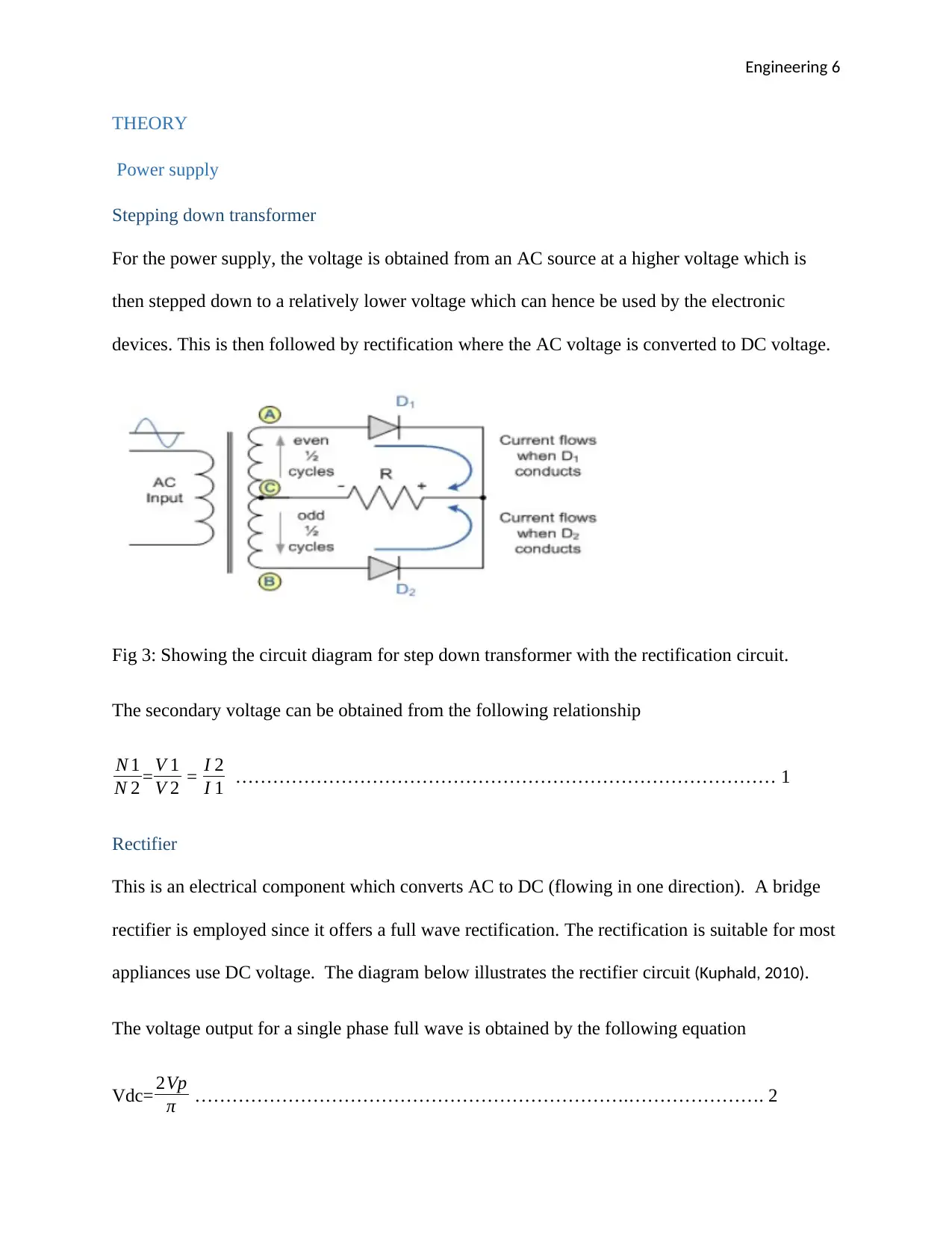
THEORY
Power supply
Stepping down transformer
For the power supply, the voltage is obtained from an AC source at a higher voltage which is
then stepped down to a relatively lower voltage which can hence be used by the electronic
devices. This is then followed by rectification where the AC voltage is converted to DC voltage.
Fig 3: Showing the circuit diagram for step down transformer with the rectification circuit.
The secondary voltage can be obtained from the following relationship
N 1
N 2 = V 1
V 2 = I 2
I 1 …………………………………………………………………………… 1
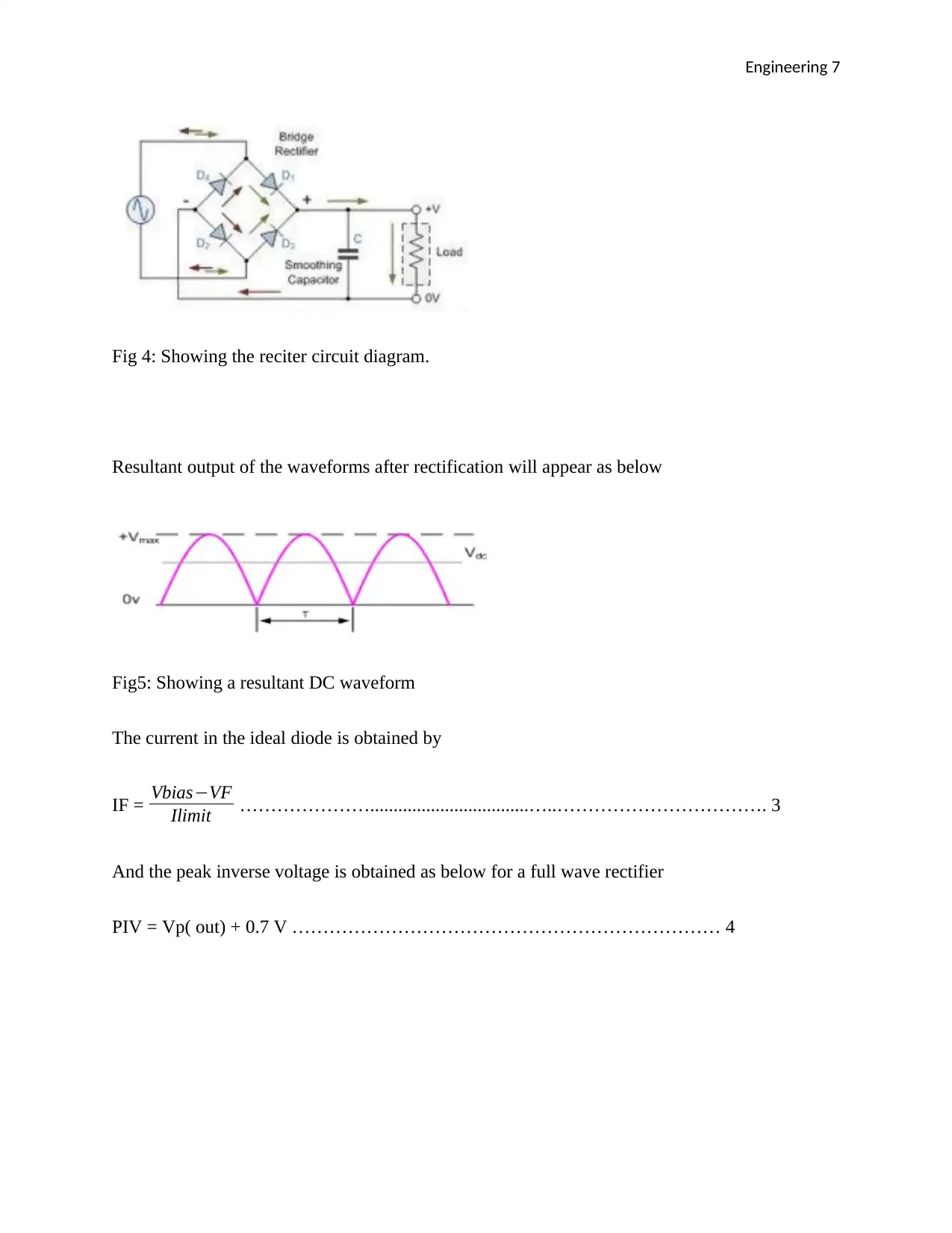
Rectifier
This is an electrical component which converts AC to DC (flowing in one direction). A bridge
rectifier is employed since it offers a full wave rectification. The rectification is suitable for most
appliances use DC voltage. The diagram below illustrates the rectifier circuit (Kuphald, 2010).
The voltage output for a single phase full wave is obtained by the following equation
Vdc= 2Vp
π …………………………………………………………….…………………. 2
THEORY
Power supply
Stepping down transformer
For the power supply, the voltage is obtained from an AC source at a higher voltage which is
then stepped down to a relatively lower voltage which can hence be used by the electronic
devices. This is then followed by rectification where the AC voltage is converted to DC voltage.
Fig 3: Showing the circuit diagram for step down transformer with the rectification circuit.
The secondary voltage can be obtained from the following relationship
N 1
N 2 = V 1
V 2 = I 2
I 1 …………………………………………………………………………… 1
Rectifier
This is an electrical component which converts AC to DC (flowing in one direction). A bridge
rectifier is employed since it offers a full wave rectification. The rectification is suitable for most
appliances use DC voltage. The diagram below illustrates the rectifier circuit (Kuphald, 2010).
The voltage output for a single phase full wave is obtained by the following equation
Vdc= 2Vp
π …………………………………………………………….…………………. 2
⊘ This is a preview!⊘
Do you want full access?
Subscribe today to unlock all pages.
Trusted by 1+ million students worldwide
Engineering 7
Fig 4: Showing the reciter circuit diagram.
Resultant output of the waveforms after rectification will appear as below
Fig5: Showing a resultant DC waveform
The current in the ideal diode is obtained by
IF = Vbias−VF
Ilimit …………………..................................…..……………………………. 3
And the peak inverse voltage is obtained as below for a full wave rectifier
PIV = Vp( out) + 0.7 V …………………………………………………………… 4
Paraphrase This Document
Need a fresh take? Get an instant paraphrase of this document with our AI Paraphraser
Engineering 8
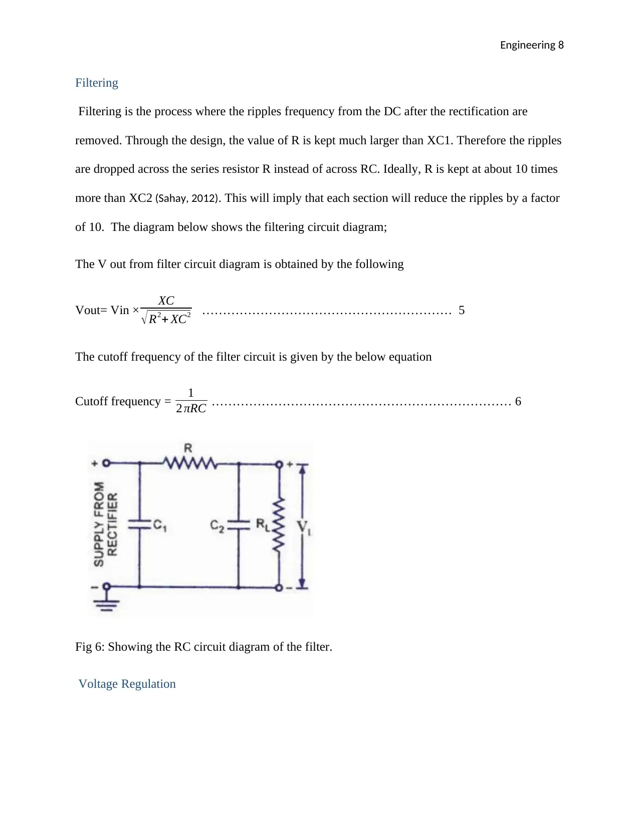
Filtering
Filtering is the process where the ripples frequency from the DC after the rectification are
removed. Through the design, the value of R is kept much larger than XC1. Therefore the ripples
are dropped across the series resistor R instead of across RC. Ideally, R is kept at about 10 times
more than XC2 (Sahay, 2012). This will imply that each section will reduce the ripples by a factor
of 10. The diagram below shows the filtering circuit diagram;
The V out from filter circuit diagram is obtained by the following
Vout= Vin × XC
√ R2+ XC2 …………………………………………………… 5
The cutoff frequency of the filter circuit is given by the below equation
Cutoff frequency = 1
2 πRC ……………………………………………………………… 6
Fig 6: Showing the RC circuit diagram of the filter.
Voltage Regulation
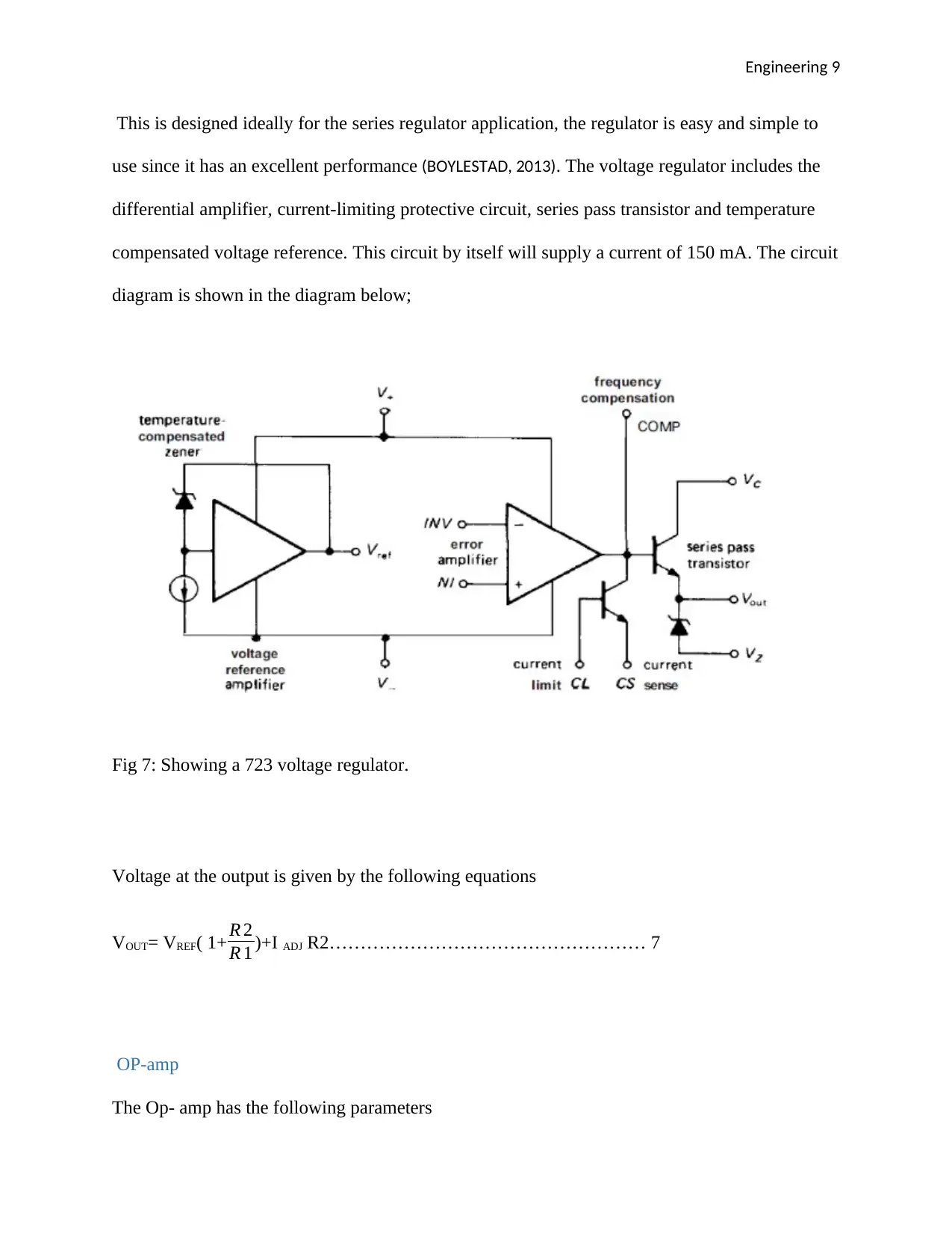
Engineering 9
This is designed ideally for the series regulator application, the regulator is easy and simple to
use since it has an excellent performance (BOYLESTAD, 2013). The voltage regulator includes the
differential amplifier, current-limiting protective circuit, series pass transistor and temperature
compensated voltage reference. This circuit by itself will supply a current of 150 mA. The circuit
diagram is shown in the diagram below;
Fig 7: Showing a 723 voltage regulator.
Voltage at the output is given by the following equations
VOUT= VREF( 1+ R 2
R 1 )+I ADJ R2…………………………………………… 7
OP-amp
The Op- amp has the following parameters
⊘ This is a preview!⊘
Do you want full access?
Subscribe today to unlock all pages.
Trusted by 1+ million students worldwide
Engineering 10
a. The Op-amp should have an infinite open loop gain: This is the gain of the Op-amp
without any feedback ( positive or negative). Hence the gain will be infinite but ideally,
those values range from 20,000 to 200,000.
b. Input Impedance (Zin) should be infinite: The input impededance for ideal amplifiers are
taken to be infinite in order to avoid any current signal flowing into amplifier input from
source supply.
c. Output impedance ( Zout) should be zero: Zout for the ideal amplifiers are taken to be
zero , this is to avoid any resistance at the output so that the amplifier may supply more
current to the output
d. Bandwidth (BW) should be infinite: An ideal Op-amp is assumed to have an infinite
bandwidth so that it can operate within a very large frequency response which can run
from a DC to AC.
e. Output Voltage should be zero: The output voltage of the amplifier is assumed to be zero
if the voltage difference between the non-inverting inputs and inverting the inputs is zero
and the same case may be witnessed if the inputs are both grounded.
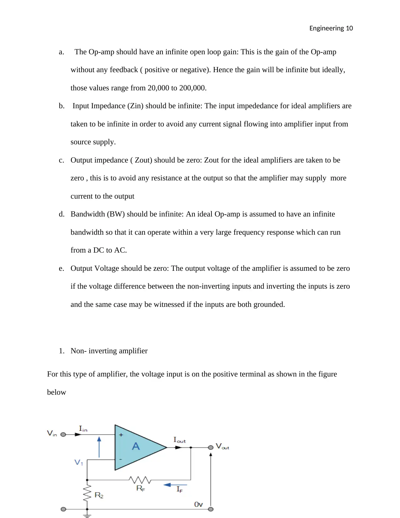
1. Non- inverting amplifier
For this type of amplifier, the voltage input is on the positive terminal as shown in the figure
below
a. The Op-amp should have an infinite open loop gain: This is the gain of the Op-amp
without any feedback ( positive or negative). Hence the gain will be infinite but ideally,
those values range from 20,000 to 200,000.
b. Input Impedance (Zin) should be infinite: The input impededance for ideal amplifiers are
taken to be infinite in order to avoid any current signal flowing into amplifier input from
source supply.
c. Output impedance ( Zout) should be zero: Zout for the ideal amplifiers are taken to be
zero , this is to avoid any resistance at the output so that the amplifier may supply more
current to the output
d. Bandwidth (BW) should be infinite: An ideal Op-amp is assumed to have an infinite
bandwidth so that it can operate within a very large frequency response which can run
from a DC to AC.
e. Output Voltage should be zero: The output voltage of the amplifier is assumed to be zero
if the voltage difference between the non-inverting inputs and inverting the inputs is zero
and the same case may be witnessed if the inputs are both grounded.
1. Non- inverting amplifier
For this type of amplifier, the voltage input is on the positive terminal as shown in the figure
below
Paraphrase This Document
Need a fresh take? Get an instant paraphrase of this document with our AI Paraphraser
Engineering 11
The voltage gain for this is given as below;
A= Vout
Vin = 1+ Rf
Rin ………………………………………………………………………… 8
The calculation revolves around the reality that the voltage at both inputs is treated to be the
same. This originates from the idea of the gain of the amplifier is very high. When the output of
the circuit is kept within the supply of the amplifier, then the output voltage divided by the gain
indicates there is no difference between the two inputs (Bose, 2014).
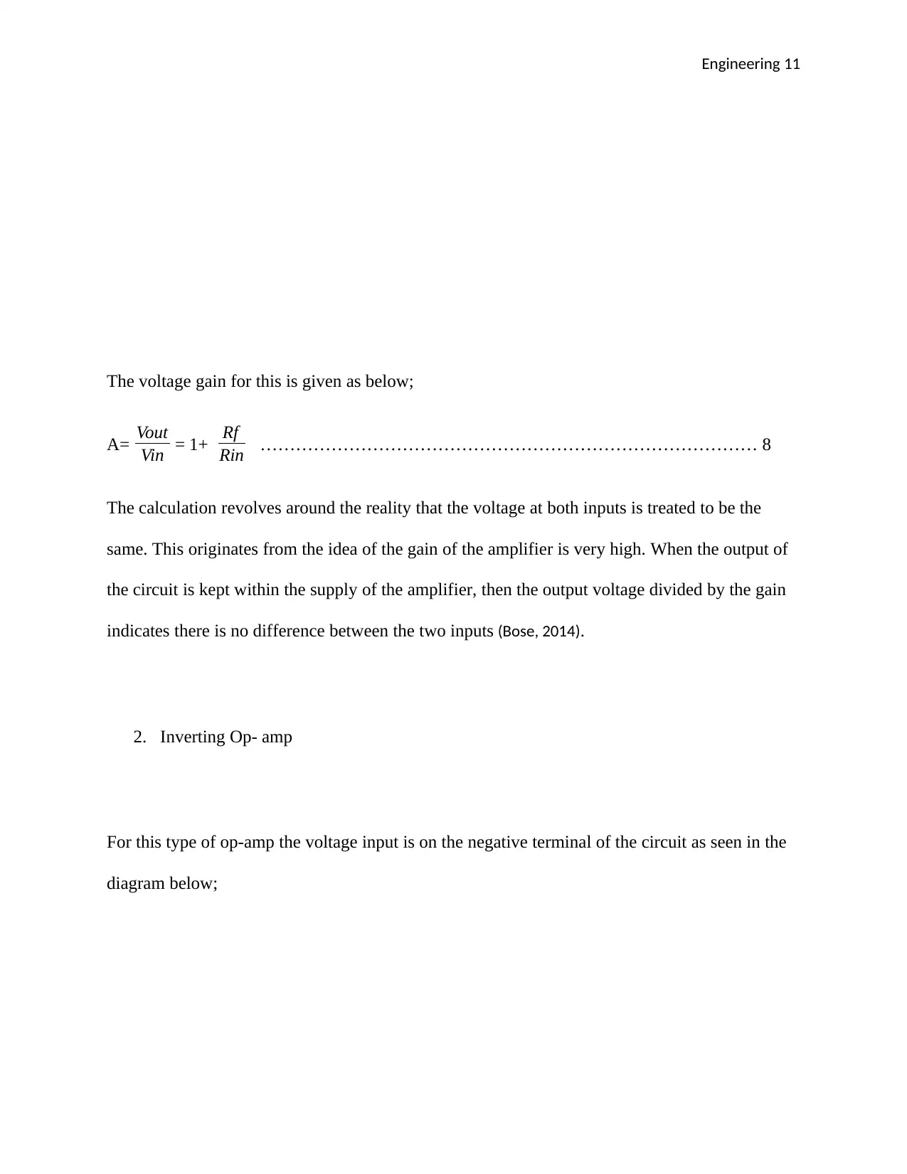
2. Inverting Op- amp
For this type of op-amp the voltage input is on the negative terminal of the circuit as seen in the
diagram below;
The voltage gain for this is given as below;
A= Vout
Vin = 1+ Rf
Rin ………………………………………………………………………… 8
The calculation revolves around the reality that the voltage at both inputs is treated to be the
same. This originates from the idea of the gain of the amplifier is very high. When the output of
the circuit is kept within the supply of the amplifier, then the output voltage divided by the gain
indicates there is no difference between the two inputs (Bose, 2014).
2. Inverting Op- amp
For this type of op-amp the voltage input is on the negative terminal of the circuit as seen in the
diagram below;
Engineering 12
This amplifier is a superior case of the where non-inverting input circuit V2 is earthed but
inverting input V1 is recognized with Vin above.
And the voltage gain (A) is given as below;
A=−Vout
Vin = - Rf
Rin ………………………………………………………………… 9
3. Differential amplifier
For the differential amplifiers , there is dissimilarity between two voltages making this amplifier
to be Subtractor amplifier, contrasting a summing amplifier which adds the input voltages (Boke,
2013). Through connecting each input in turn to 0v we can use superposition to obtain the output
voltage Vout.
⊘ This is a preview!⊘
Do you want full access?
Subscribe today to unlock all pages.
Trusted by 1+ million students worldwide
1 out of 33
Related Documents


Your All-in-One AI-Powered Toolkit for Academic Success.
+13062052269
info@desklib.com
Available 24*7 on WhatsApp / Email
![[object Object]](/_next/static/media/star-bottom.7253800d.svg)
Unlock your academic potential
Copyright © 2020–2026 A2Z Services. All Rights Reserved. Developed and managed by ZUCOL.