Analysis of Transistor Amplifiers and Logic Circuits in Electronics
VerifiedAdded on 2023/01/18
|17
|1906
|56
Homework Assignment
AI Summary
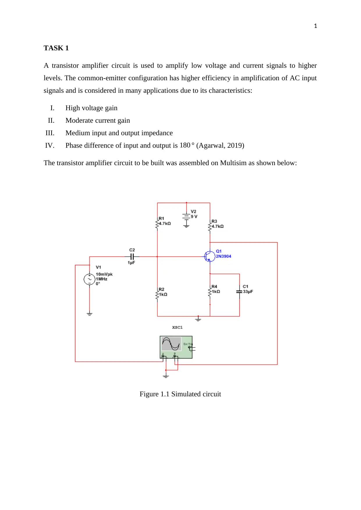
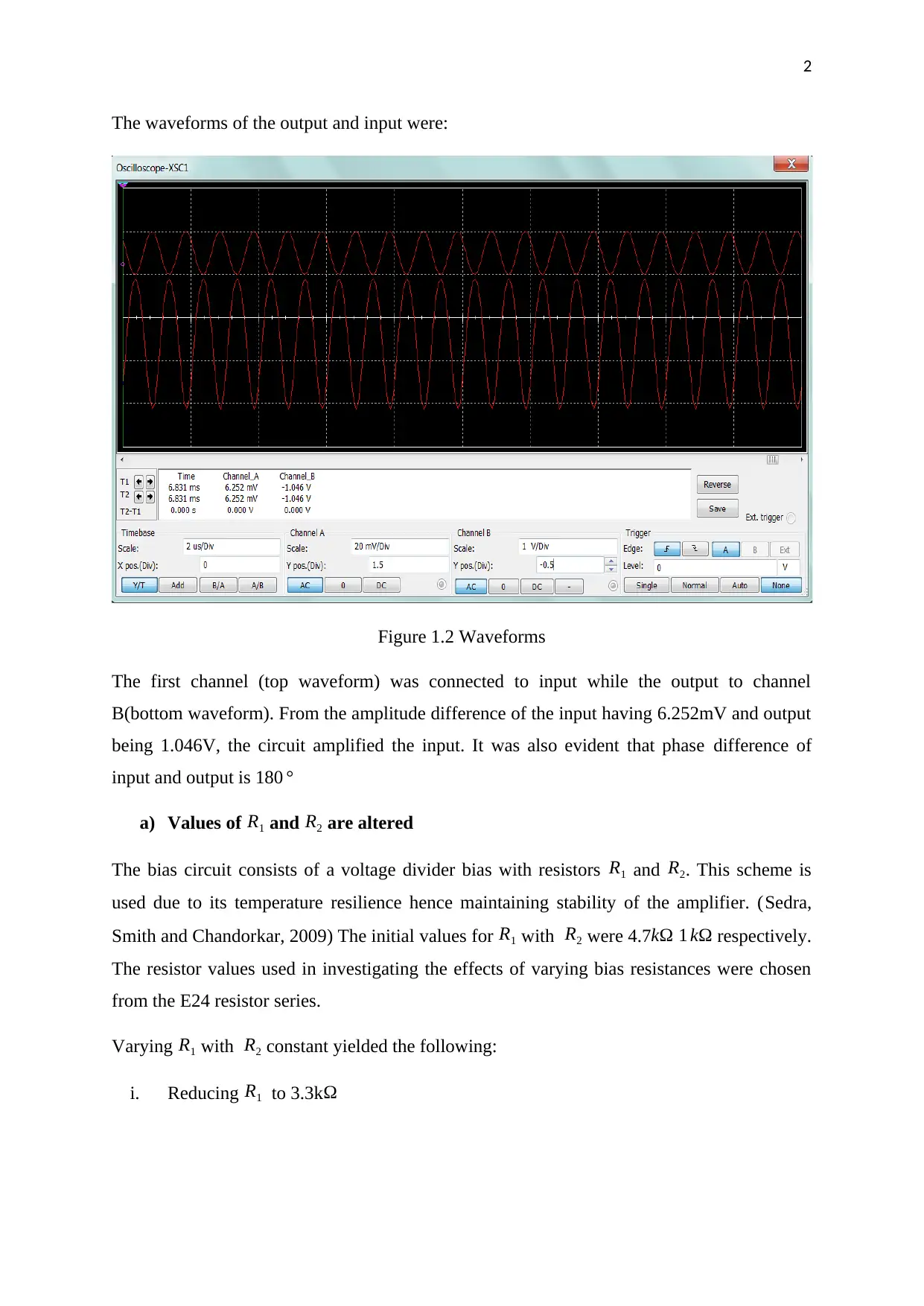
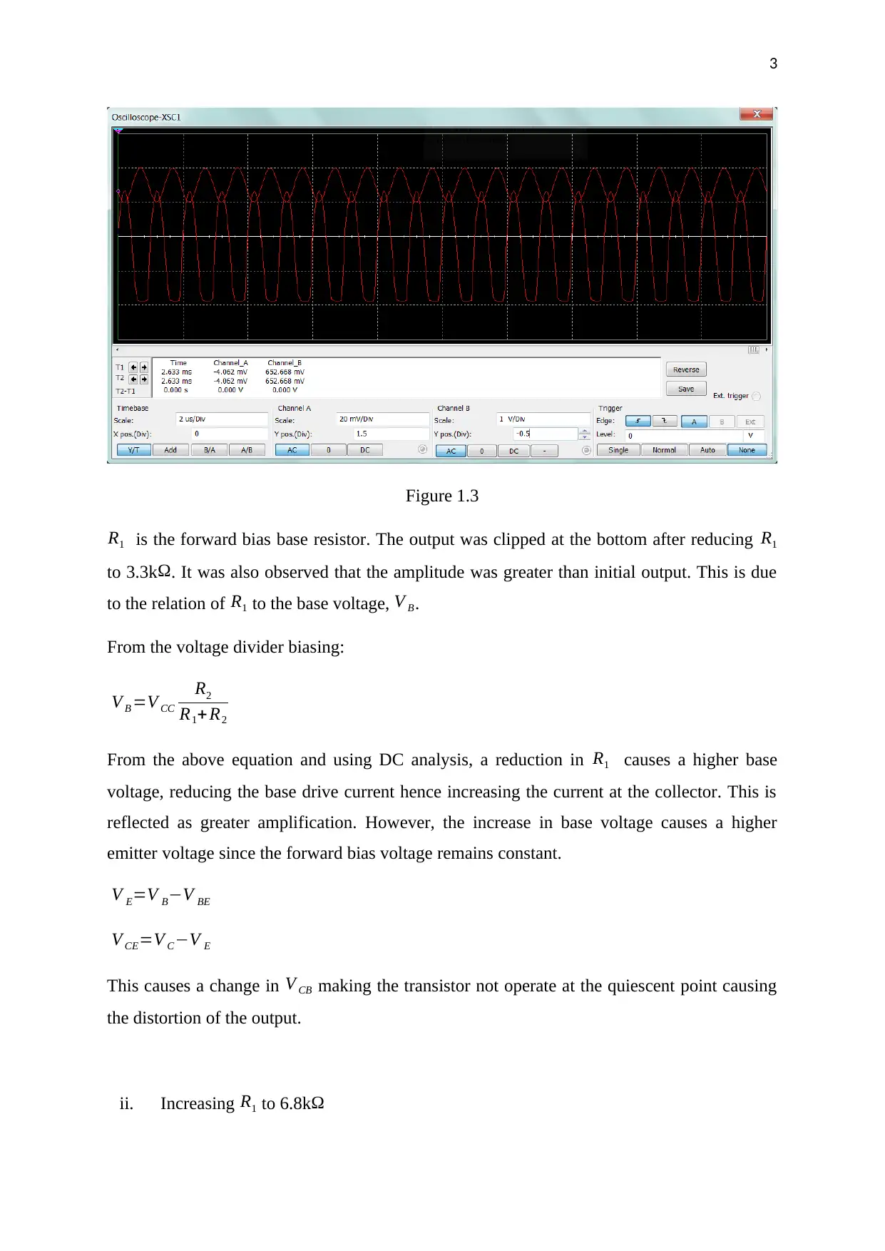
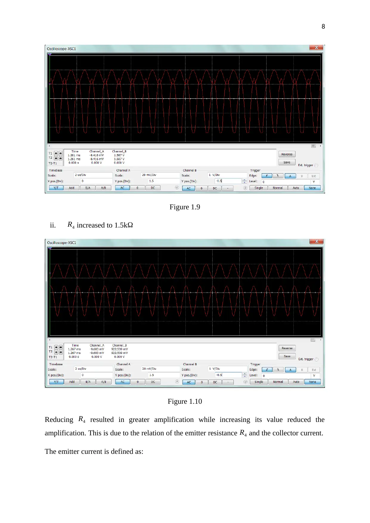
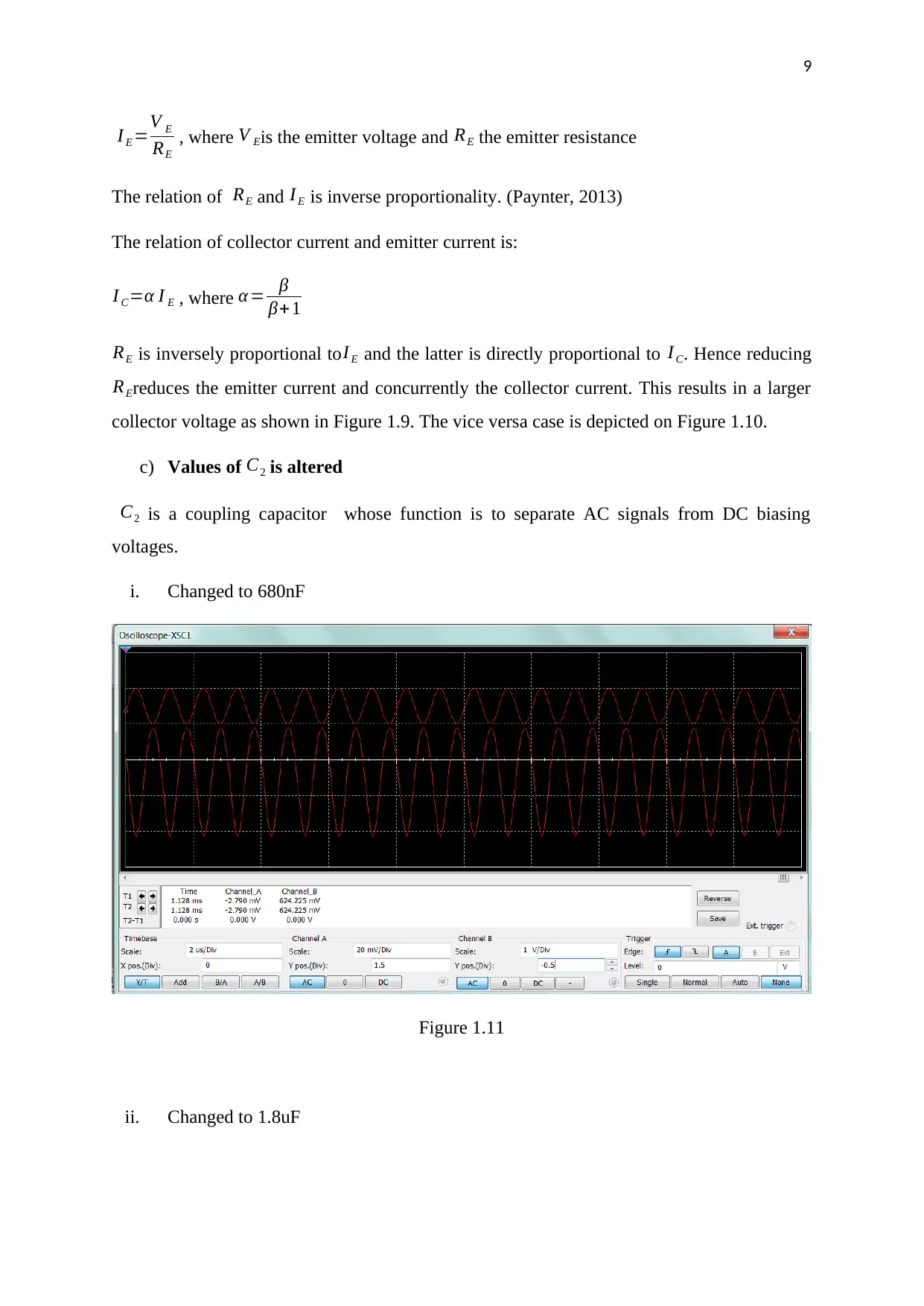
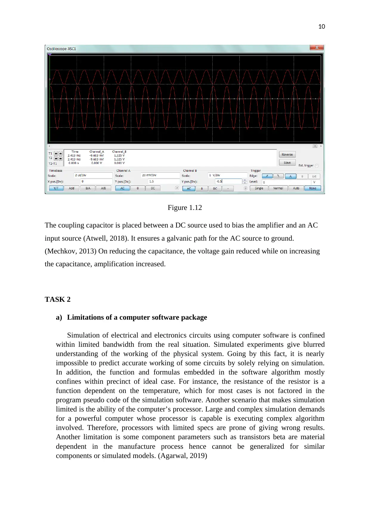
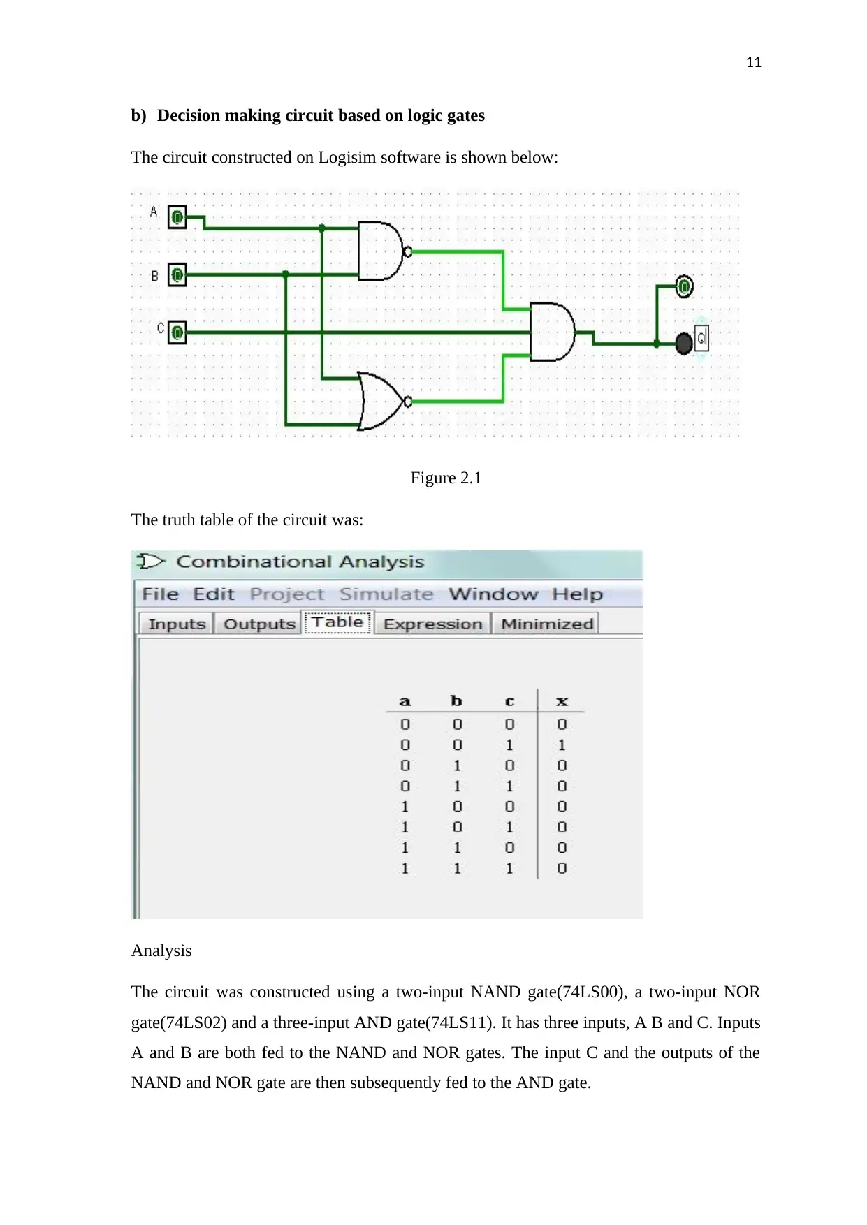
This assignment delves into the principles and applications of electronic devices and circuits. The first task focuses on analyzing a transistor amplifier circuit in a common-emitter configuration, exploring the effects of varying resistor and capacitor values on voltage gain and output characteristics through Multisim simulations. The analysis includes detailed explanations of how changes in bias resistors (R1 and R2), load resistance (R3), emitter resistance (R4), and coupling capacitor (C2) impact the amplifier's performance, including voltage gain and phase shift. The second task explores the limitations of computer software packages in simulating electronic circuits and provides a detailed analysis of a decision-making circuit built using logic gates (NAND, NOR, and AND), including a truth table and Boolean expression. Finally, the assignment covers the design and simulation of a 5-volt DC power supply, detailing the components (transformer, rectifier, smoothing circuit, and regulator) and presenting simulation results to confirm its functionality. The document concludes with a comprehensive list of cited works.

Student
Professor
Principles and applications of Electronic Devices and Circuits
Date
Professor
Principles and applications of Electronic Devices and Circuits
Date
Paraphrase This Document
Need a fresh take? Get an instant paraphrase of this document with our AI Paraphraser

1
TASK 1
A transistor amplifier circuit is used to amplify low voltage and current signals to higher
levels. The common-emitter configuration has higher efficiency in amplification of AC input
signals and is considered in many applications due to its characteristics:
I. High voltage gain
II. Moderate current gain
III. Medium input and output impedance
IV. Phase difference of input and output is 180 ° (Agarwal, 2019)
The transistor amplifier circuit to be built was assembled on Multisim as shown below:
Figure 1.1 Simulated circuit

2
The waveforms of the output and input were:
Figure 1.2 Waveforms
The first channel (top waveform) was connected to input while the output to channel
B(bottom waveform). From the amplitude difference of the input having 6.252mV and output
being 1.046V, the circuit amplified the input. It was also evident that phase difference of
input and output is 180 °
a) Values of R1 and R2 are altered
The bias circuit consists of a voltage divider bias with resistors R1 and R2. This scheme is
used due to its temperature resilience hence maintaining stability of the amplifier. (Sedra,
Smith and Chandorkar, 2009) The initial values for R1 with R2 were 4.7kΩ 1 kΩ respectively.
The resistor values used in investigating the effects of varying bias resistances were chosen
from the E24 resistor series.
Varying R1 with R2 constant yielded the following:
i. Reducing R1 to 3.3kΩ
⊘ This is a preview!⊘
Do you want full access?
Subscribe today to unlock all pages.

Trusted by 1+ million students worldwide

3
Figure 1.3
R1 is the forward bias base resistor. The output was clipped at the bottom after reducing R1
to 3.3kΩ. It was also observed that the amplitude was greater than initial output. This is due
to the relation of R1 to the base voltage, V B.
From the voltage divider biasing:
V B =V CC
R2
R1+ R2
From the above equation and using DC analysis, a reduction in R1 causes a higher base
voltage, reducing the base drive current hence increasing the current at the collector. This is
reflected as greater amplification. However, the increase in base voltage causes a higher
emitter voltage since the forward bias voltage remains constant.
V E=V B−V BE
V CE=V C−V E
This causes a change in V CB making the transistor not operate at the quiescent point causing
the distortion of the output.
ii. Increasing R1 to 6.8kΩ
Paraphrase This Document
Need a fresh take? Get an instant paraphrase of this document with our AI Paraphraser

4
Figure 1.4
Increasing R1 to 6.8kΩ will reduce the voltage of the base:
V B =V CC
R2
R1+ R2
From DC analysis, this will increase the base drive current of the transistor thereby reducing
the collector current.(Leach, 2010) The result is lower amplification as seen in the image
above.
Varying R2with R1 constant yielded the following:
i. Reducing R2 to 680Ω

5
Figure 1.5
R2 is the resistance that develops the bias for the base. Its relation to the base voltage is:
V B =V CC
R2
R1+ R2
R2 is proportional to the voltage of the base hence a reduction in R2 causes a decrease in
amplification.
ii. Increasing R2 to 1.5kΩ
Figure 1.5
R2 is the resistance that develops the bias for the base. Its relation to the base voltage is:
V B =V CC
R2
R1+ R2
R2 is proportional to the voltage of the base hence a reduction in R2 causes a decrease in
amplification.
ii. Increasing R2 to 1.5kΩ
⊘ This is a preview!⊘
Do you want full access?
Subscribe today to unlock all pages.

Trusted by 1+ million students worldwide

6
Figure 1.6
An increase in R2 causes an increase in forward bias resulting in greater amplification
b) Values of R3 and R4 are altered
R3 is the load resistance.
i. R3 reduced to 3.3kΩ
Figure 1.7
The forward current gain of a common emitter amplifier is:
β= Δ I C
Δ I B
The voltage gain is:
Av=β R3
RB
, where RB is the input resistance
From the voltage gain relation, R3 is proportional to voltage gain. Hence a decrease in R3
caused a decrease in voltage gain.
ii. R3 increased to 6.8k Ω
Paraphrase This Document
Need a fresh take? Get an instant paraphrase of this document with our AI Paraphraser

7
Figure 1.8
From the voltage gain equation,
Av=β R3
RB
, where RB is the input resistance
R3 is proportional to voltage gain. Hence a increase in R3 caused a increase in voltage gain as
shown on the image above.
R4 is the emitter resistance
i. R4 reduced to 680Ω
Figure 1.8
From the voltage gain equation,
Av=β R3
RB
, where RB is the input resistance
R3 is proportional to voltage gain. Hence a increase in R3 caused a increase in voltage gain as
shown on the image above.
R4 is the emitter resistance
i. R4 reduced to 680Ω

8
Figure 1.9
ii. R4 increased to 1.5kΩ
Figure 1.10
Reducing R4 resulted in greater amplification while increasing its value reduced the
amplification. This is due to the relation of the emitter resistance R4 and the collector current.
The emitter current is defined as:
Figure 1.9
ii. R4 increased to 1.5kΩ
Figure 1.10
Reducing R4 resulted in greater amplification while increasing its value reduced the
amplification. This is due to the relation of the emitter resistance R4 and the collector current.
The emitter current is defined as:
⊘ This is a preview!⊘
Do you want full access?
Subscribe today to unlock all pages.

Trusted by 1+ million students worldwide

9
I E =V E
RE
, where V Eis the emitter voltage and RE the emitter resistance
The relation of RE and I E is inverse proportionality. (Paynter, 2013)
The relation of collector current and emitter current is:
I C=α I E , where α = β
β+ 1
RE is inversely proportional to I E and the latter is directly proportional to I C. Hence reducing
REreduces the emitter current and concurrently the collector current. This results in a larger
collector voltage as shown in Figure 1.9. The vice versa case is depicted on Figure 1.10.
c) Values of C2 is altered
C2 is a coupling capacitor whose function is to separate AC signals from DC biasing
voltages.
i. Changed to 680nF
Figure 1.11
ii. Changed to 1.8uF
Paraphrase This Document
Need a fresh take? Get an instant paraphrase of this document with our AI Paraphraser

10
Figure 1.12
The coupling capacitor is placed between a DC source used to bias the amplifier and an AC
input source (Atwell, 2018). It ensures a galvanic path for the AC source to ground.
(Mechkov, 2013) On reducing the capacitance, the voltage gain reduced while on increasing
the capacitance, amplification increased.
TASK 2
a) Limitations of a computer software package
Simulation of electrical and electronics circuits using computer software is confined
within limited bandwidth from the real situation. Simulated experiments give blurred
understanding of the working of the physical system. Going by this fact, it is nearly
impossible to predict accurate working of some circuits by solely relying on simulation.
In addition, the function and formulas embedded in the software algorithm mostly
confines within precinct of ideal case. For instance, the resistance of the resistor is a
function dependent on the temperature, which for most cases is not factored in the
program pseudo code of the simulation software. Another scenario that makes simulation
limited is the ability of the computer’s processor. Large and complex simulation demands
for a powerful computer whose processor is capable is executing complex algorithm
involved. Therefore, processors with limited specs are prone of giving wrong results.
Another limitation is some component parameters such as transistors beta are material
dependent in the manufacture process hence cannot be generalized for similar
components or simulated models. (Agarwal, 2019)

11
b) Decision making circuit based on logic gates
The circuit constructed on Logisim software is shown below:
Figure 2.1
The truth table of the circuit was:
Analysis
The circuit was constructed using a two-input NAND gate(74LS00), a two-input NOR
gate(74LS02) and a three-input AND gate(74LS11). It has three inputs, A B and C. Inputs
A and B are both fed to the NAND and NOR gates. The input C and the outputs of the
NAND and NOR gate are then subsequently fed to the AND gate.
⊘ This is a preview!⊘
Do you want full access?
Subscribe today to unlock all pages.

Trusted by 1+ million students worldwide
1 out of 17
Related Documents

Your All-in-One AI-Powered Toolkit for Academic Success.
+13062052269
info@desklib.com
Available 24*7 on WhatsApp / Email
Unlock your academic potential
Copyright © 2020–2025 A2Z Services. All Rights Reserved. Developed and managed by ZUCOL.