Teesside University: Programmable Logic Controllers Assignment
VerifiedAdded on 2022/08/12
|18
|2302
|21
Homework Assignment
AI Summary
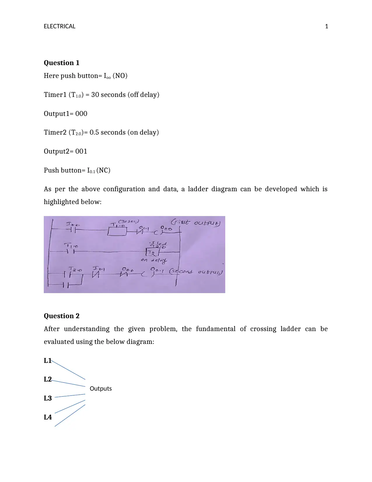
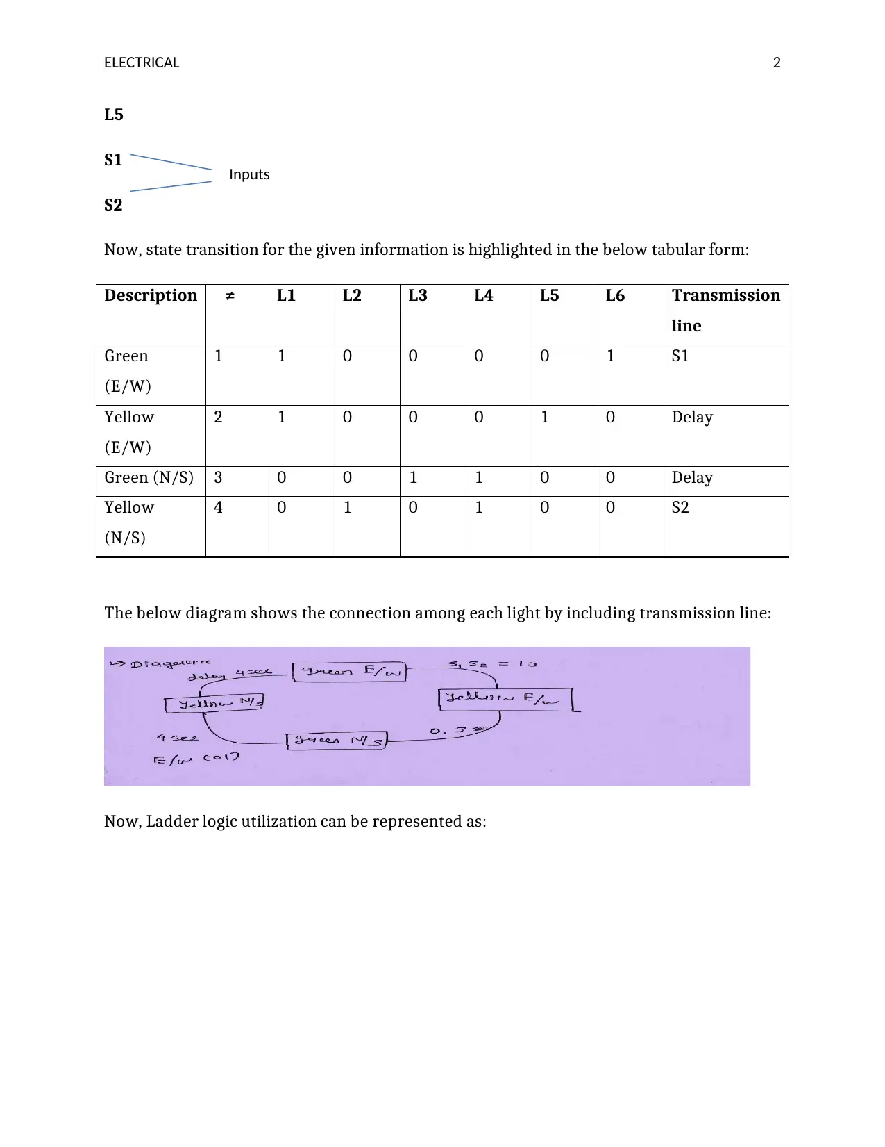
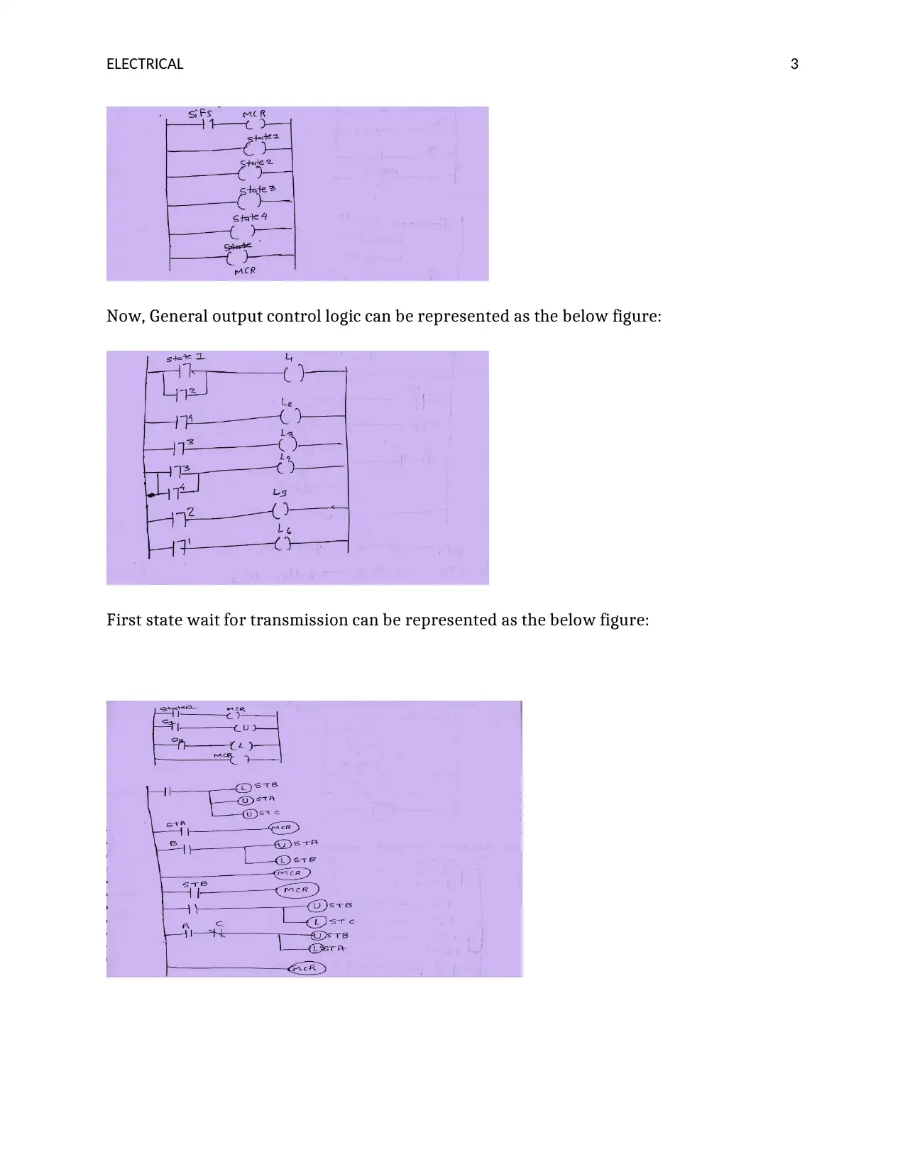
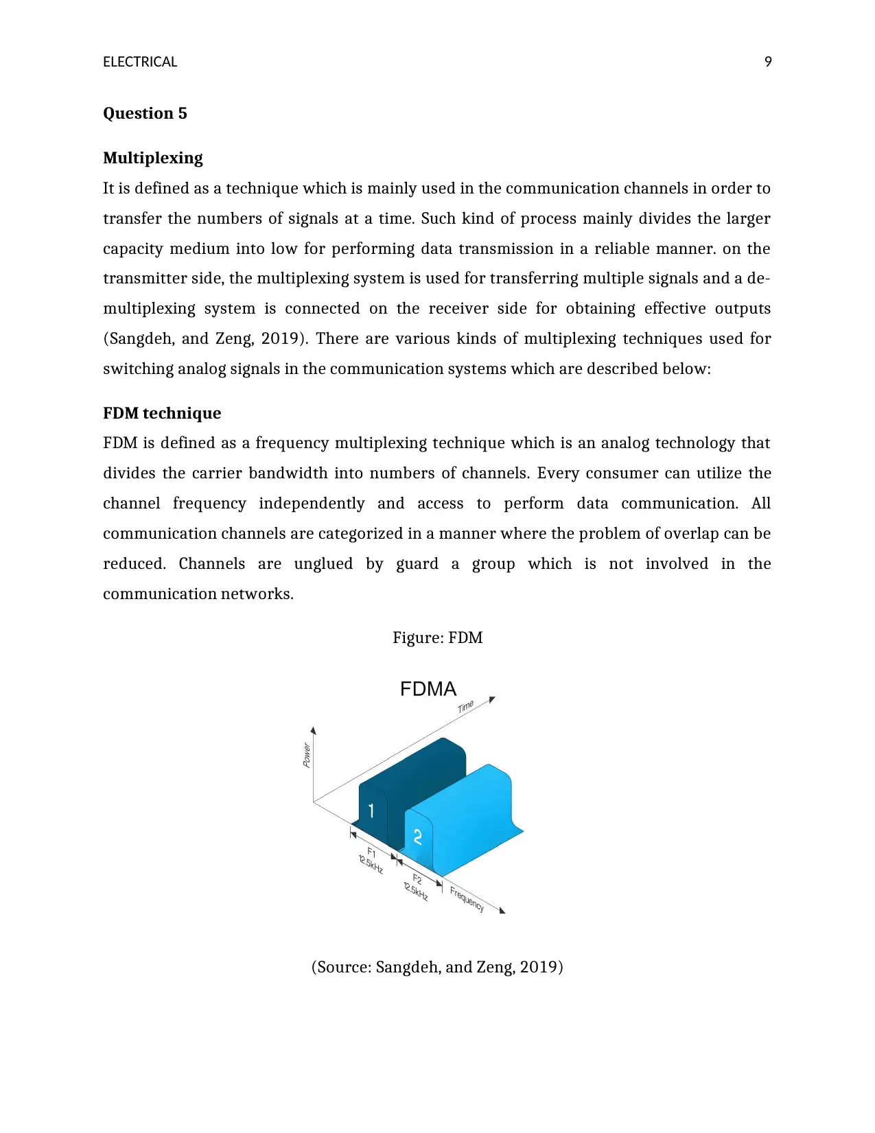
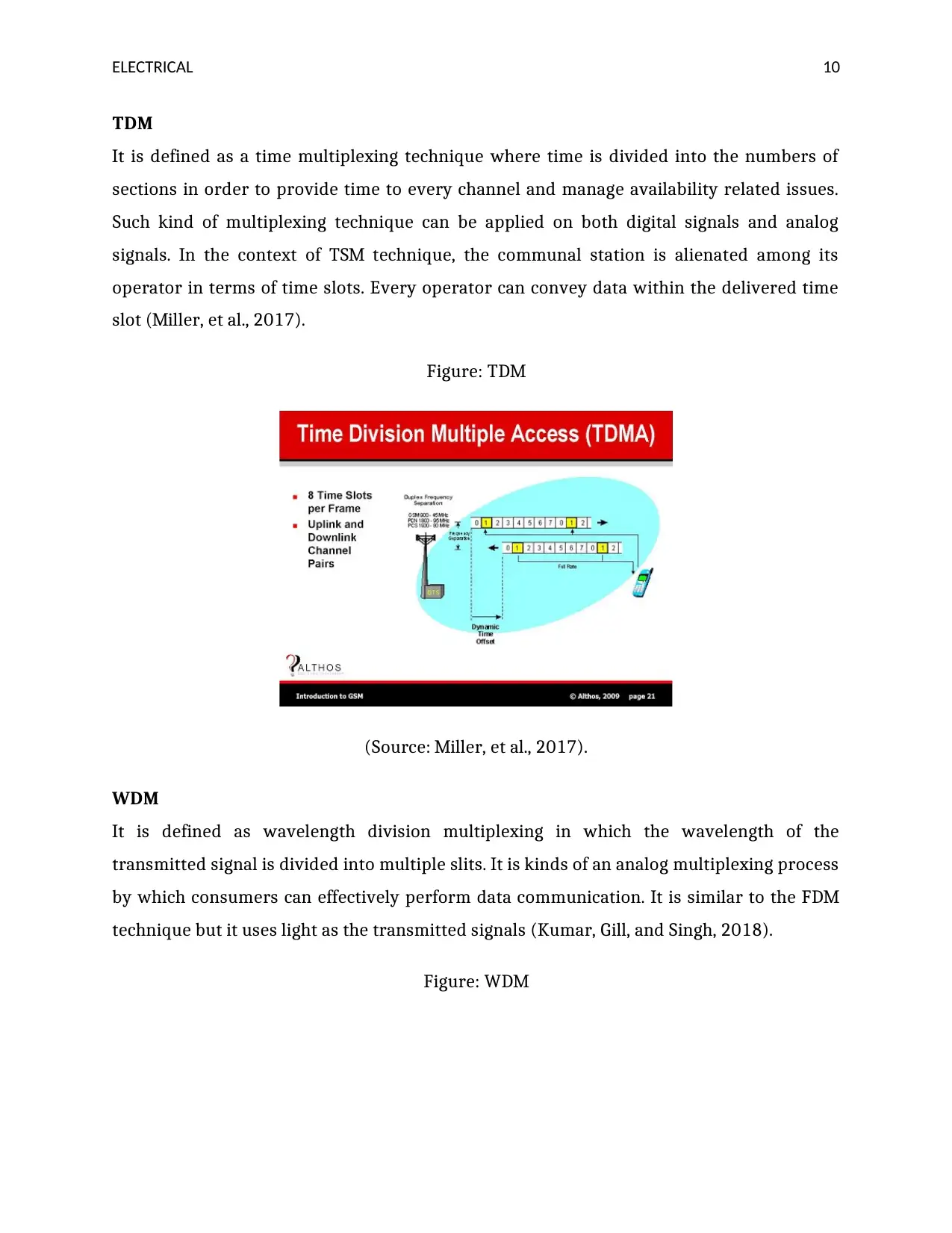
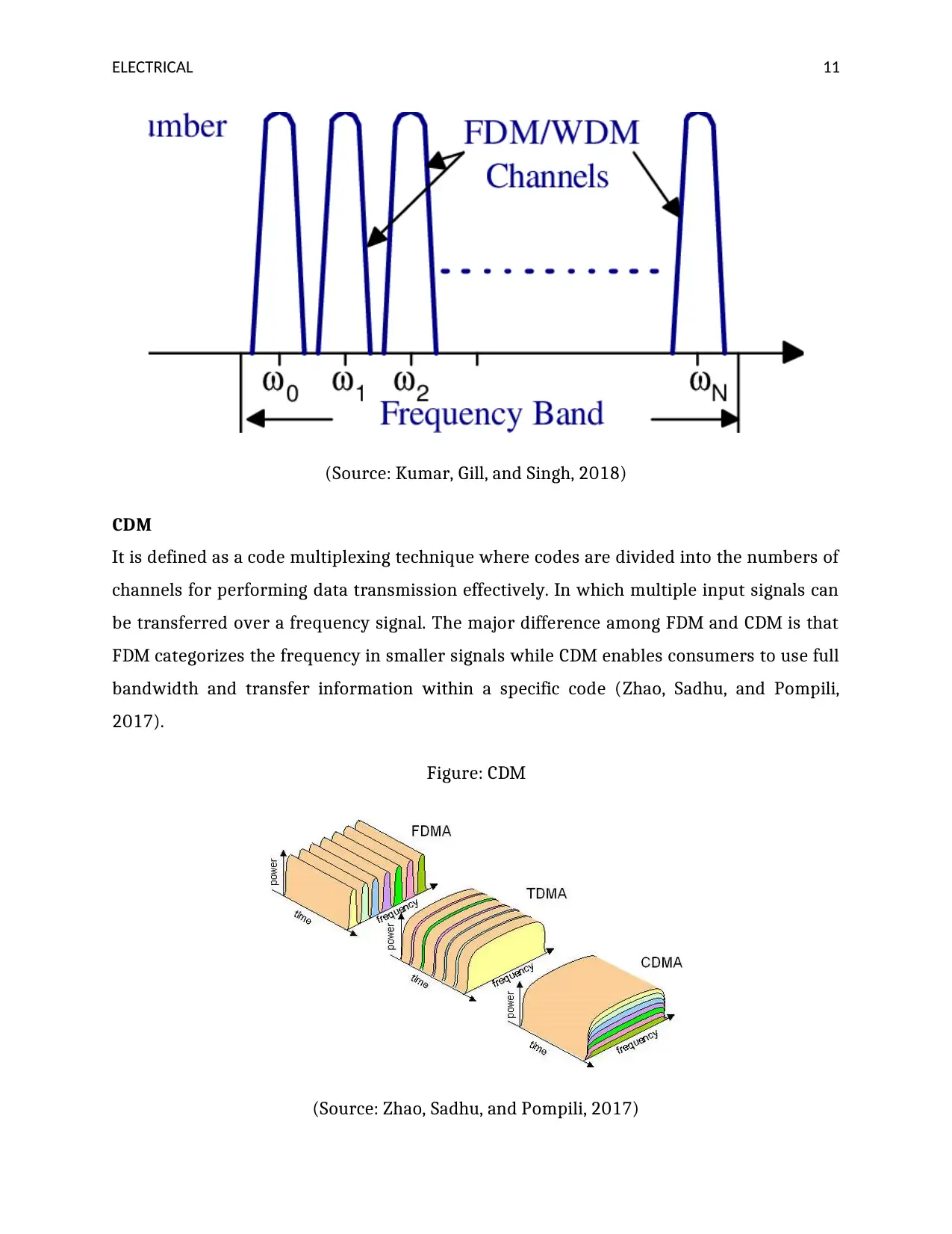
This document presents a complete solution to a Programmable Logic Controllers (PLC) assignment, addressing multiple facets of PLC programming and related technologies. The solution begins with a ladder diagram implementation based on given specifications, including timer functionalities and output controls. It then explores state transition diagrams and boolean expressions for traffic light control systems. The assignment further delves into shift register applications, detailing the control of relays using 8-bit shift registers. Additionally, the solution analyzes A/D conversion, calculating bit resolutions and converting decimal to hexadecimal values. The document also covers multiplexing techniques (FDM, TDM, WDM, and CDM), and the application of these techniques in communication systems. Finally, the assignment addresses circuit analysis, LAN applications, and the functionalities of RTUs, EIA-422, and IEEE-488 standards. The solution incorporates references to support the concepts discussed.

ELECTRICAL 0
PROGRAMMABLE LOGIC
CONTROLLERS
PROGRAMMABLE LOGIC
CONTROLLERS
Paraphrase This Document
Need a fresh take? Get an instant paraphrase of this document with our AI Paraphraser

ELECTRICAL 1
Question 1
Here push button= Ioo (NO)
Timer1 (T1.0) = 30 seconds (off delay)
Output1= 000
Timer2 (T2.0)= 0.5 seconds (on delay)
Output2= 001
Push button= I0.1 (NC)
As per the above configuration and data, a ladder diagram can be developed which is
highlighted below:
Question 2
After understanding the given problem, the fundamental of crossing ladder can be
evaluated using the below diagram:
L1
L2
L3
L4
Outputs

ELECTRICAL 2
L5
S1
S2
Now, state transition for the given information is highlighted in the below tabular form:
Description ≠ L1 L2 L3 L4 L5 L6 Transmission
line
Green
(E/W)
1 1 0 0 0 0 1 S1
Yellow
(E/W)
2 1 0 0 0 1 0 Delay
Green (N/S) 3 0 0 1 1 0 0 Delay
Yellow
(N/S)
4 0 1 0 1 0 0 S2
The below diagram shows the connection among each light by including transmission line:
Now, Ladder logic utilization can be represented as:
Inputs
⊘ This is a preview!⊘
Do you want full access?
Subscribe today to unlock all pages.

Trusted by 1+ million students worldwide

ELECTRICAL 3
Now, General output control logic can be represented as the below figure:
First state wait for transmission can be represented as the below figure:
Now, General output control logic can be represented as the below figure:
First state wait for transmission can be represented as the below figure:
Paraphrase This Document
Need a fresh take? Get an instant paraphrase of this document with our AI Paraphraser

ELECTRICAL 4
Here, ST1 is state1 used for green signal (N/S), ST2 is called as state2 which is used for
yellow (N/S), ST3 represents state3 which is used for green (E/W) and ST4 is state4 which
is used to represent yellow (E/W).
Now, simplifying boolean expressions of all states can provide to draw ladder diagram
which are highlighted below:
ST1= [ST1+ ST4(TON2)*(ST4*4)]*(ST1+ S1+ S2)+ Fs
ST2= (ST2+ ST1- S1*S2)*(ST2+ TON1(ST2), 1)1
ST3= [ST3+ ST2*TON1(ST4*4)]* (ST3+ S1+ S2)
ST4= (ST4+ ST3*S1*S2)*[ST4+ TON2(ST4, 4)]
Therefore, logics for state equations can be represented as per the below figure:
The below figure shows delayed state updating in the ladder diagram:

ELECTRICAL 5
Now, output for all lights can be represented as:
Question 3
As per the given case, it is reported that there are two 8-bit shift registers where every
register has major 3 input terminals that may control the total eight relays in the system.
The below figure shows 3:8 shift register in which data is defined as input data, the clock is
used to provide clock input and RESET is used for restarting shift register. In this figure,
C50 is defined as control relay 50 and first shift register will control total 8 relays starting
⊘ This is a preview!⊘
Do you want full access?
Subscribe today to unlock all pages.

Trusted by 1+ million students worldwide

ELECTRICAL 6
from 50 to 57. Second shift register will be able to control 8-relays starting from 60 to 67.
After providing the input signal, the shift register will start from step 1 to 15 on a regular
basis. In which relay 65 is used to reset shift register-1.
The below figure show working of both shift registers as per the given input signals:
Paraphrase This Document
Need a fresh take? Get an instant paraphrase of this document with our AI Paraphraser

ELECTRICAL 7
In this entire process, relay C65 is utilized to rest 2nd Shift Register and help to provide an
input signal to first Shift Register.
Question 4
Part A
A/D with 10-bit resolution can be determined using the below equation:
5/1024= 4.88 mv/bits
In this entire process, relay C65 is utilized to rest 2nd Shift Register and help to provide an
input signal to first Shift Register.
Question 4
Part A
A/D with 10-bit resolution can be determined using the below equation:
5/1024= 4.88 mv/bits

ELECTRICAL 8
Therefore, at 2V the value will be given as:
2/4.88= 409.6 bits or 410 bits
Now, A/D with 12-bit resolution and 0-10V range is given as:
10/4096= 2.44 mv/bits
Now, for 2V:
2/2.44= 819.2 bits or 819 bits
Therefore, converting decimal into hexadecimal the data can be represented as:
410= 0*19A (Hex)
819= 0*333 (Hex)
Part B
It is examined that digital output value of an A/D converter is rarely the same digital value
as the input value due to the process of quantization that mapped larger set of input signals
in the proposed system.
Part C
It is examined that A/D converters utilize one converter system and various channels in
order to convert the analog signal into digital. Moreover, the A/D converter uses a polling
process for the analog input lines in order to poll input signals at a specific frequency. So, it
is reported that for a 4-channel analog to digital converter, the maximum on-time for any
channel is 1/4 seconds.
Part D
From part “A” it is found that the 12-bit resolution with the voltage range 0-10V is better as
compared with the 10-bit resolution as it is twice of the 10-bit signal. Moreover, in the case
of 12 bit, the resolution of the signal can be easily seen due to the larger resolution rate.
⊘ This is a preview!⊘
Do you want full access?
Subscribe today to unlock all pages.

Trusted by 1+ million students worldwide

ELECTRICAL 9
Question 5
Multiplexing
It is defined as a technique which is mainly used in the communication channels in order to
transfer the numbers of signals at a time. Such kind of process mainly divides the larger
capacity medium into low for performing data transmission in a reliable manner. on the
transmitter side, the multiplexing system is used for transferring multiple signals and a de-
multiplexing system is connected on the receiver side for obtaining effective outputs
(Sangdeh, and Zeng, 2019). There are various kinds of multiplexing techniques used for
switching analog signals in the communication systems which are described below:
FDM technique
FDM is defined as a frequency multiplexing technique which is an analog technology that
divides the carrier bandwidth into numbers of channels. Every consumer can utilize the
channel frequency independently and access to perform data communication. All
communication channels are categorized in a manner where the problem of overlap can be
reduced. Channels are unglued by guard a group which is not involved in the
communication networks.
Figure: FDM
(Source: Sangdeh, and Zeng, 2019)
Paraphrase This Document
Need a fresh take? Get an instant paraphrase of this document with our AI Paraphraser

ELECTRICAL 10
TDM
It is defined as a time multiplexing technique where time is divided into the numbers of
sections in order to provide time to every channel and manage availability related issues.
Such kind of multiplexing technique can be applied on both digital signals and analog
signals. In the context of TSM technique, the communal station is alienated among its
operator in terms of time slots. Every operator can convey data within the delivered time
slot (Miller, et al., 2017).
Figure: TDM
(Source: Miller, et al., 2017).
WDM
It is defined as wavelength division multiplexing in which the wavelength of the
transmitted signal is divided into multiple slits. It is kinds of an analog multiplexing process
by which consumers can effectively perform data communication. It is similar to the FDM
technique but it uses light as the transmitted signals (Kumar, Gill, and Singh, 2018).
Figure: WDM

ELECTRICAL 11
(Source: Kumar, Gill, and Singh, 2018)
CDM
It is defined as a code multiplexing technique where codes are divided into the numbers of
channels for performing data transmission effectively. In which multiple input signals can
be transferred over a frequency signal. The major difference among FDM and CDM is that
FDM categorizes the frequency in smaller signals while CDM enables consumers to use full
bandwidth and transfer information within a specific code (Zhao, Sadhu, and Pompili,
2017).
Figure: CDM
(Source: Zhao, Sadhu, and Pompili, 2017)
⊘ This is a preview!⊘
Do you want full access?
Subscribe today to unlock all pages.

Trusted by 1+ million students worldwide
1 out of 18
Your All-in-One AI-Powered Toolkit for Academic Success.
+13062052269
info@desklib.com
Available 24*7 on WhatsApp / Email
Unlock your academic potential
Copyright © 2020–2026 A2Z Services. All Rights Reserved. Developed and managed by ZUCOL.

