TMA3: Programmable Logic Controllers Assignment Solutions
VerifiedAdded on 2022/08/14
|20
|1447
|16
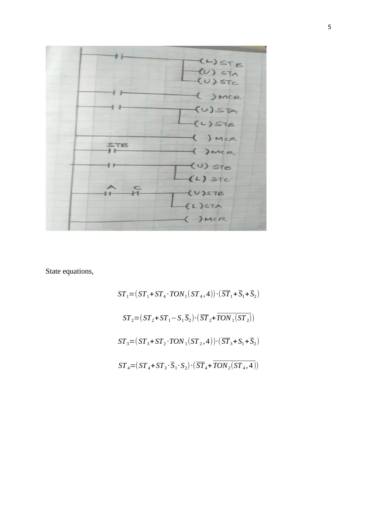
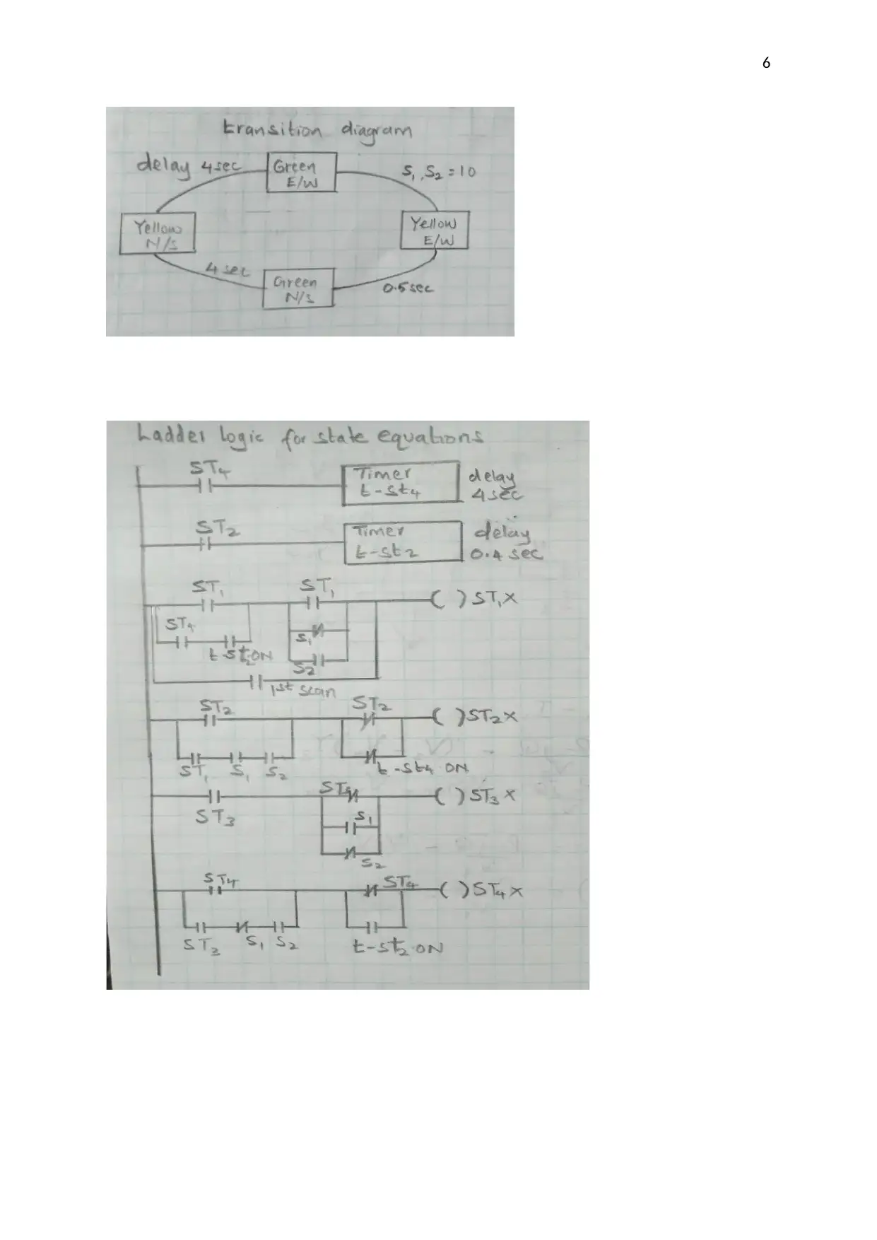
Homework Assignment
AI Summary
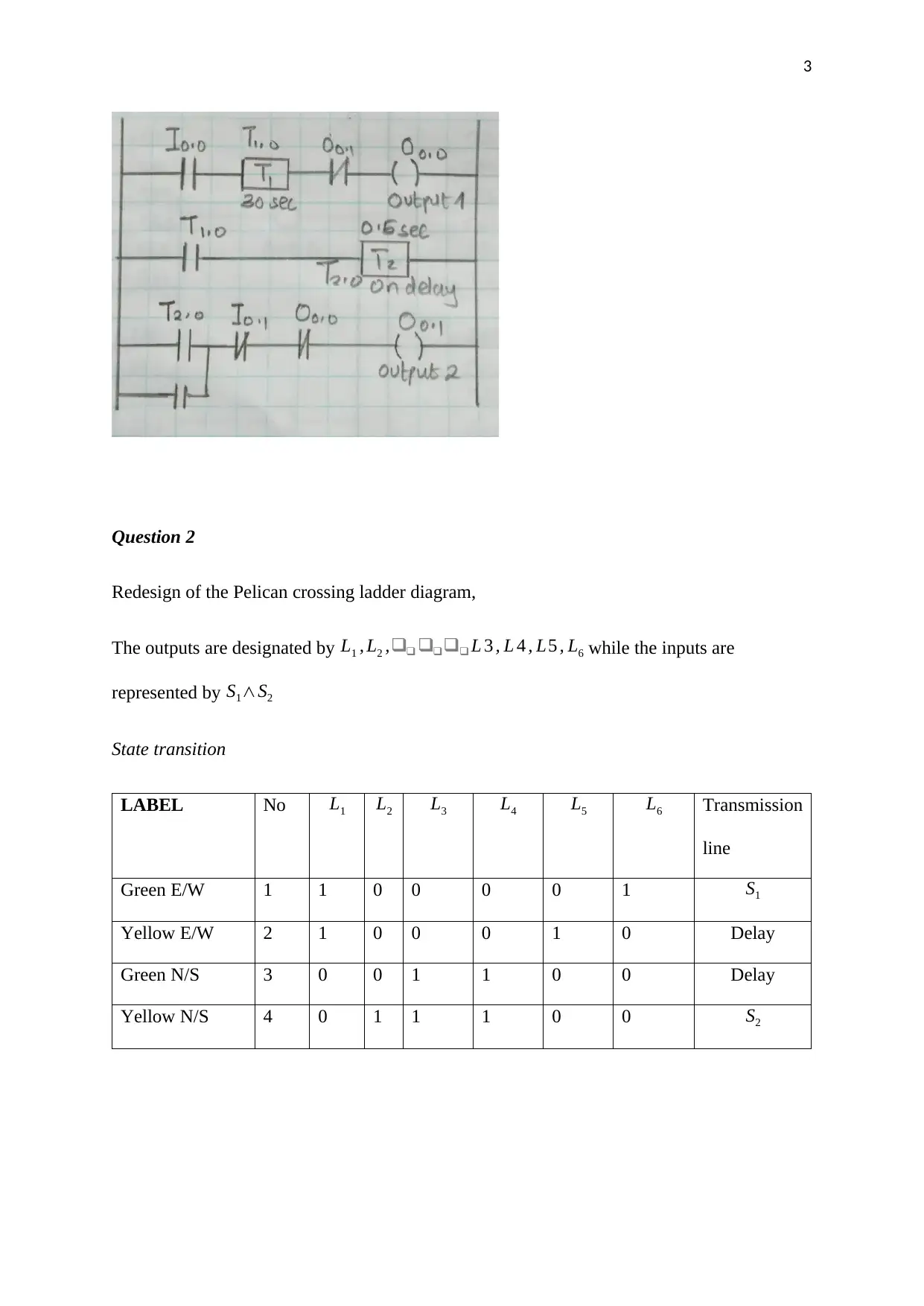
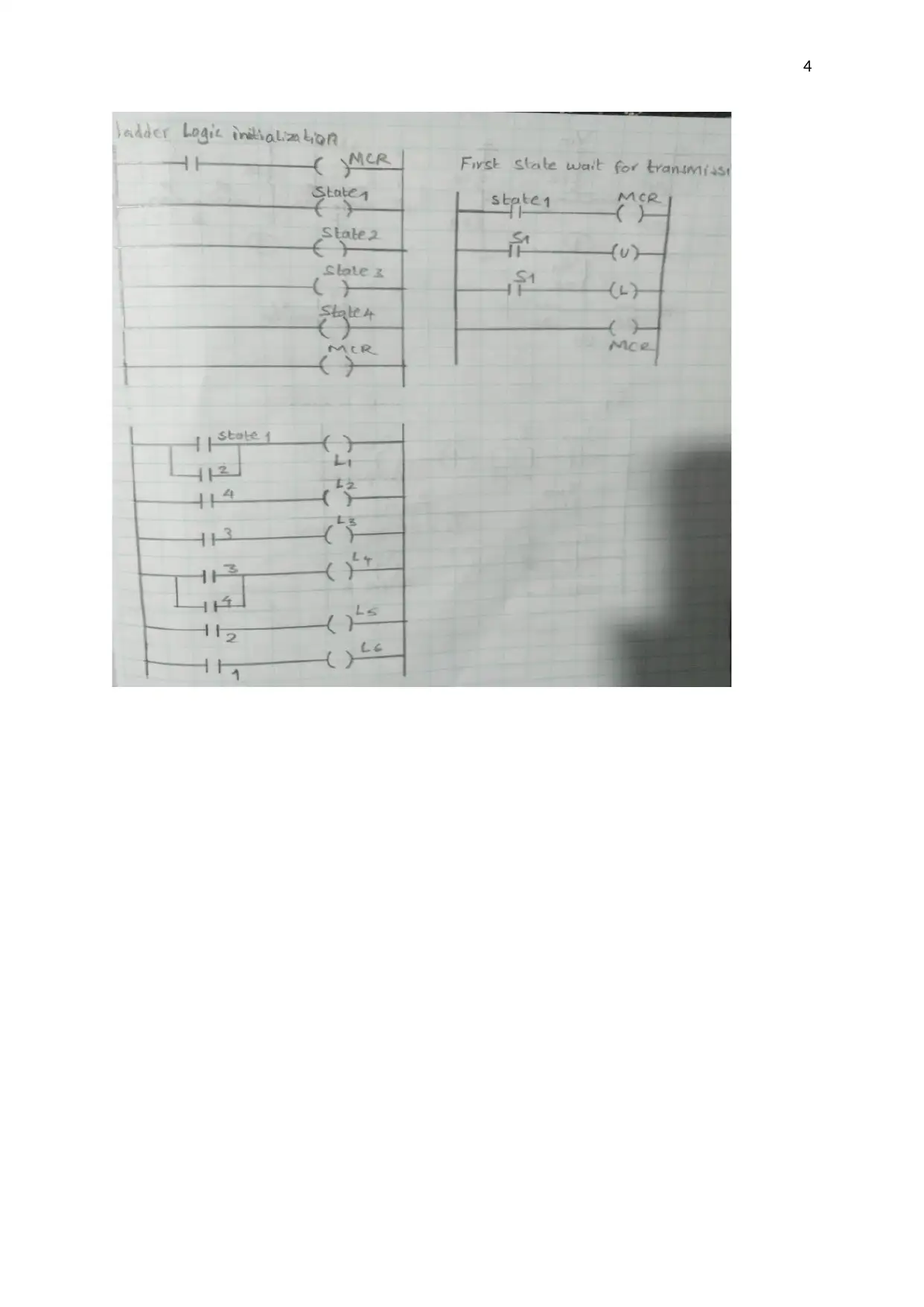
This document presents a comprehensive solution to a Programmable Logic Controller (PLC) assignment. The solution addresses various aspects of PLC programming and related concepts. Question 1 focuses on designing ladder logic diagrams for momentary pushbuttons and timers, including off-delay timers and output designations. Question 2 involves the redesign of a Pelican crossing ladder diagram, including state transition diagrams and state equations. Question 3 delves into the use of shift registers for controlling relays, outlining the initialization and operational steps. Question 4 explores analog-to-digital (A/D) conversion, including step size calculations, hexadecimal conversions, and the impact of quantization errors, as well as a comparison of converters with different resolutions. Question 5 discusses multiplexing techniques, specifically analog multiplexing, including frequency division multiplexing (FDM) and wavelength division multiplexing (WDM). Question 6 involves circuit analysis using superposition theorem. Question 7 provides an overview of Local Area Networks (LANs), including types, applications, cable types, and the definition of Remote Terminal Units (RTUs), as well as the standards EIA-422 (RS-422) and IEEE-488. The assignment covers a wide range of topics related to PLC and electrical engineering principles.
1 out of 20
Related Documents


Your All-in-One AI-Powered Toolkit for Academic Success.
+13062052269
info@desklib.com
Available 24*7 on WhatsApp / Email
![[object Object]](/_next/static/media/star-bottom.7253800d.svg)
Copyright © 2020–2026 A2Z Services. All Rights Reserved. Developed and managed by ZUCOL.