PWM Technique for D.C Motor Speed Control: Design and Implementation
VerifiedAdded on 2023/03/31
|15
|2246
|372
Report
AI Summary
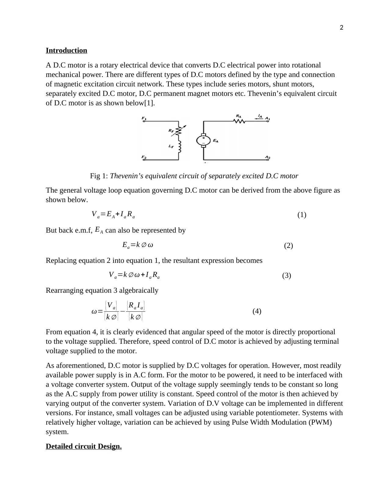
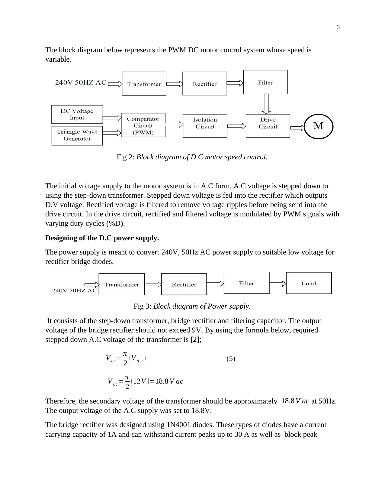
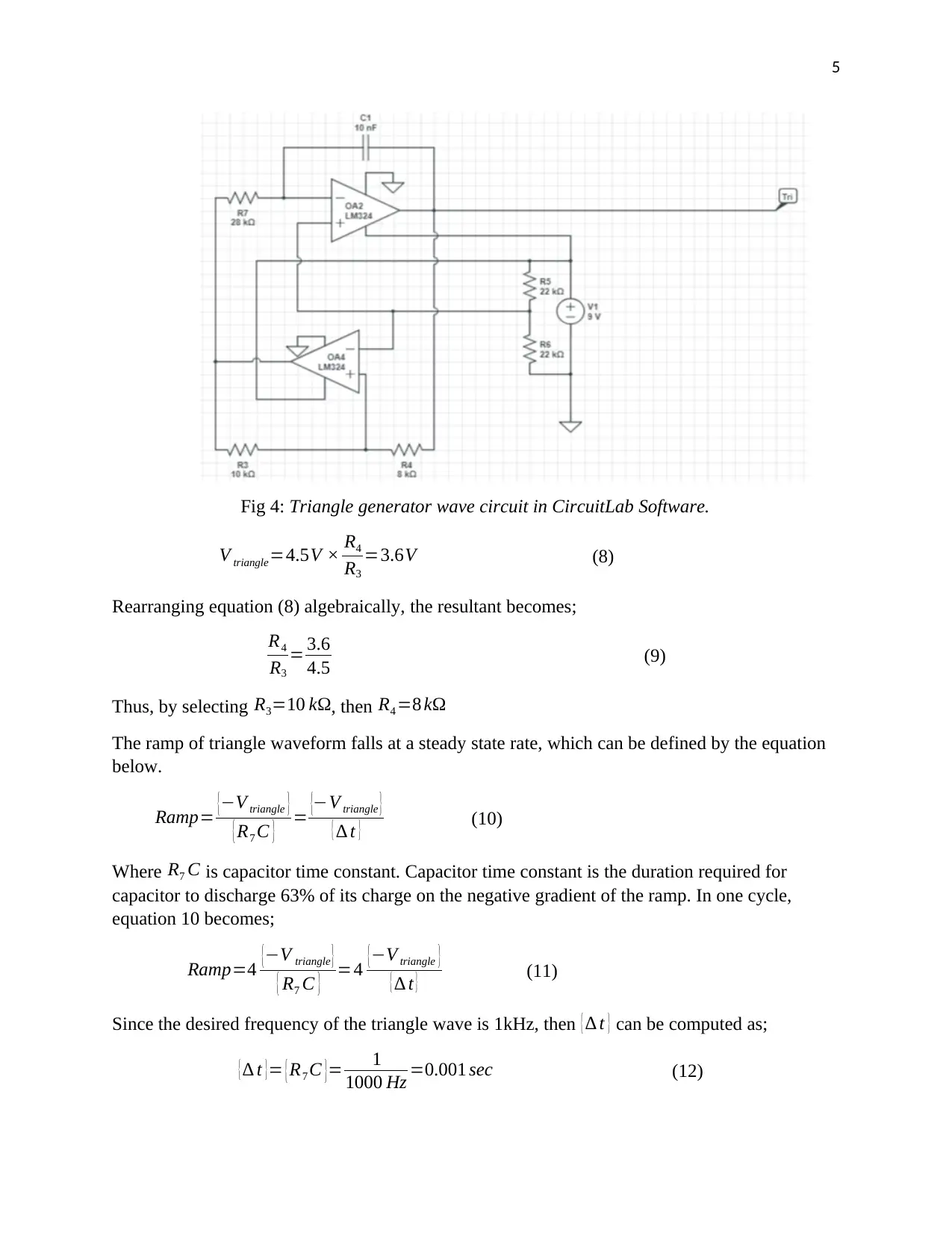
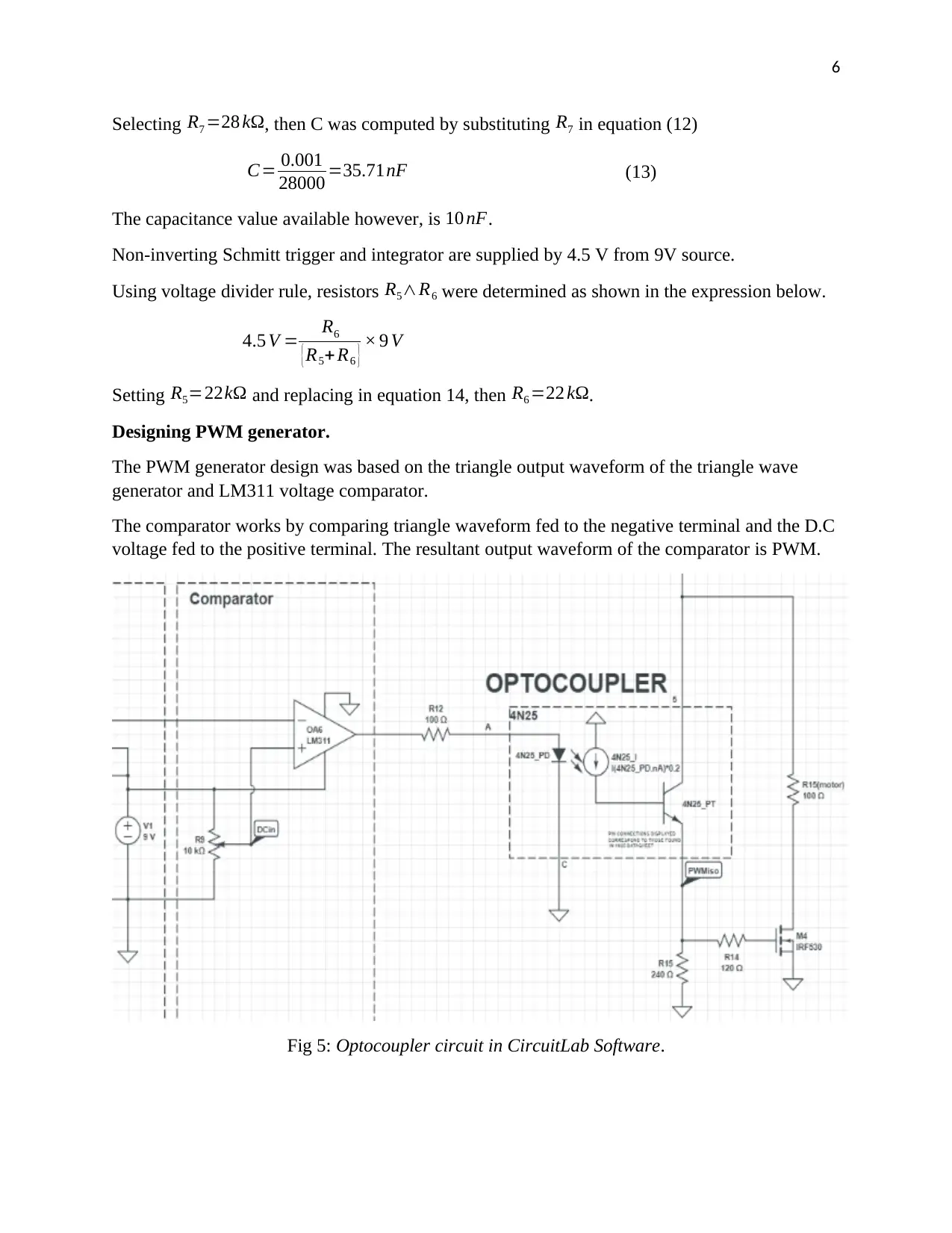
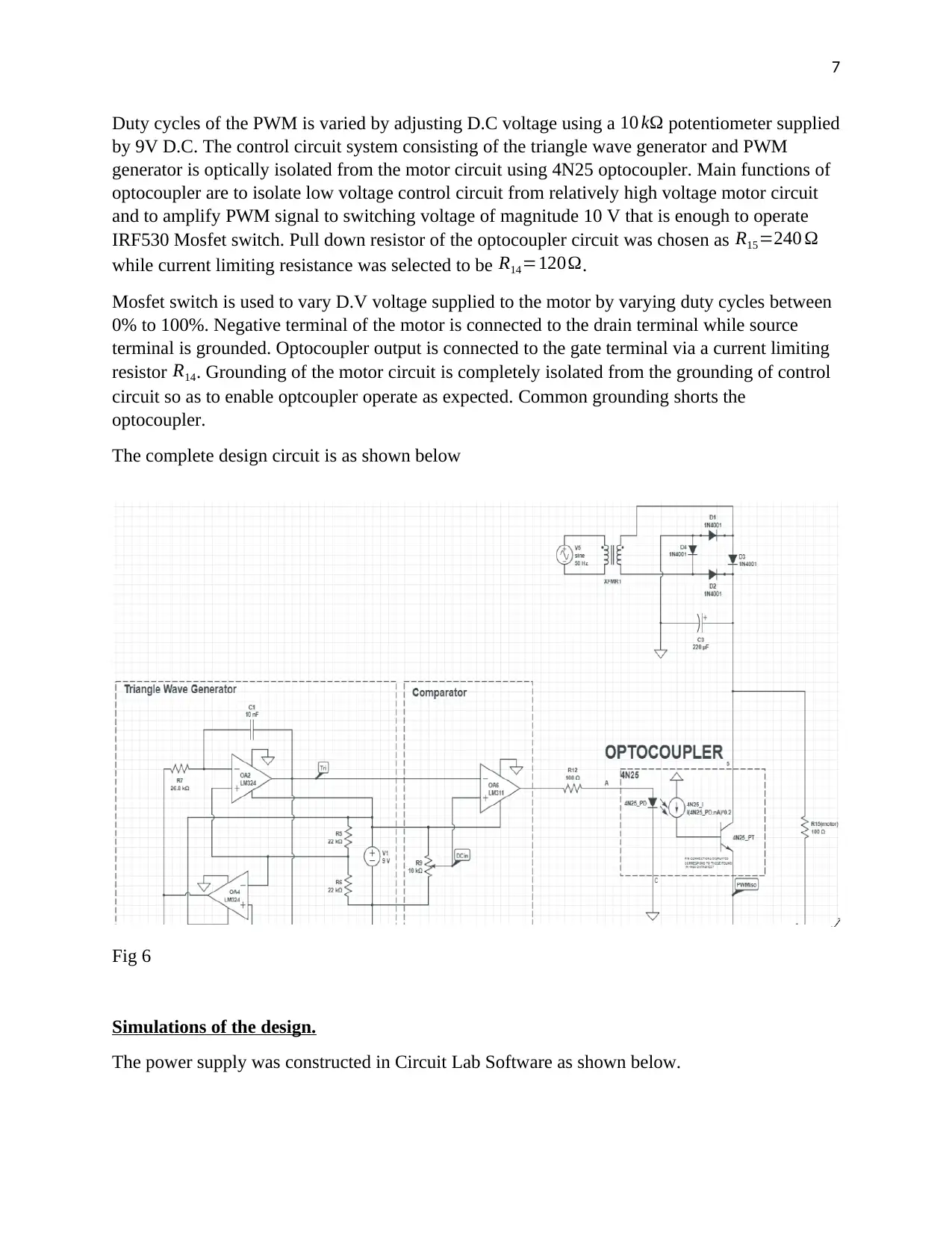
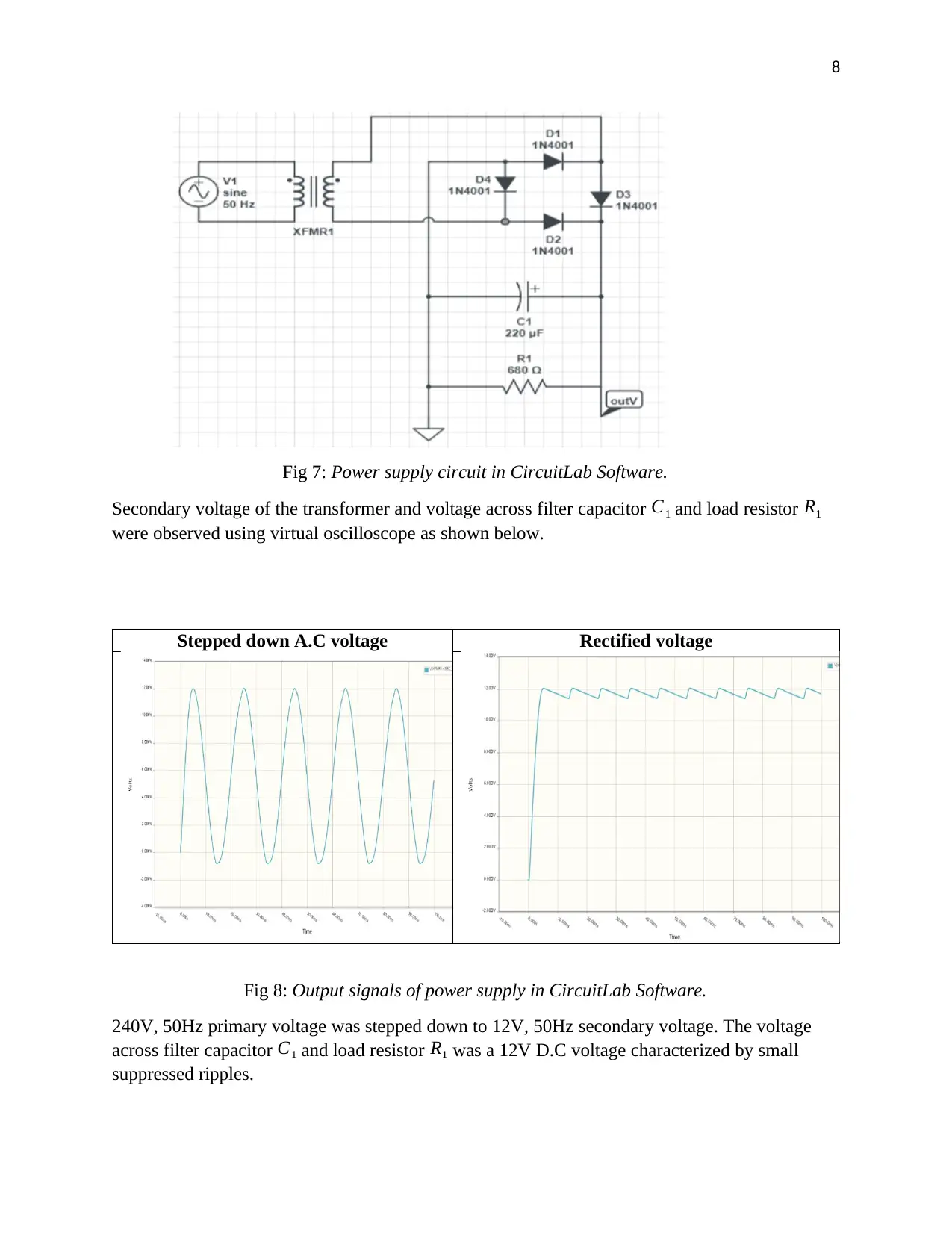
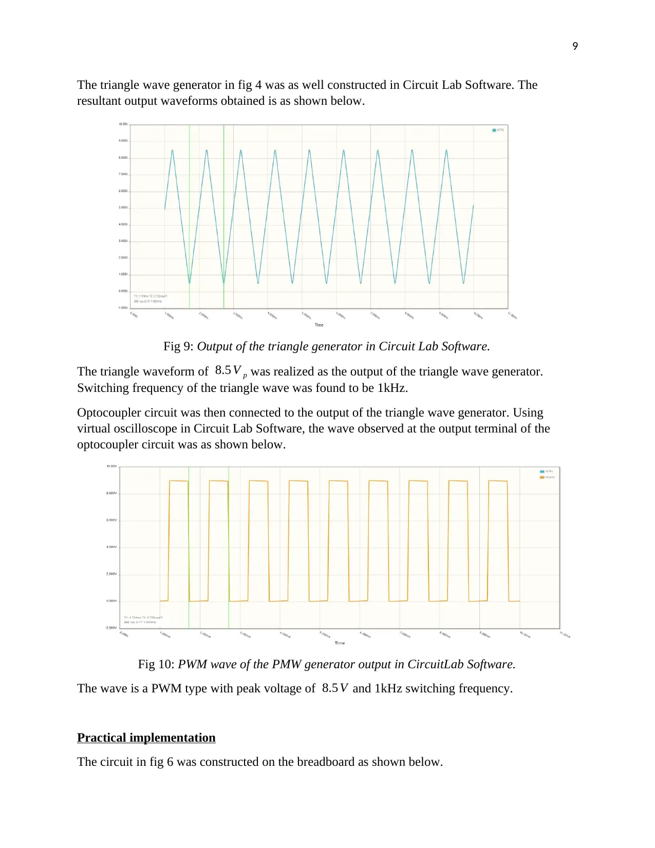
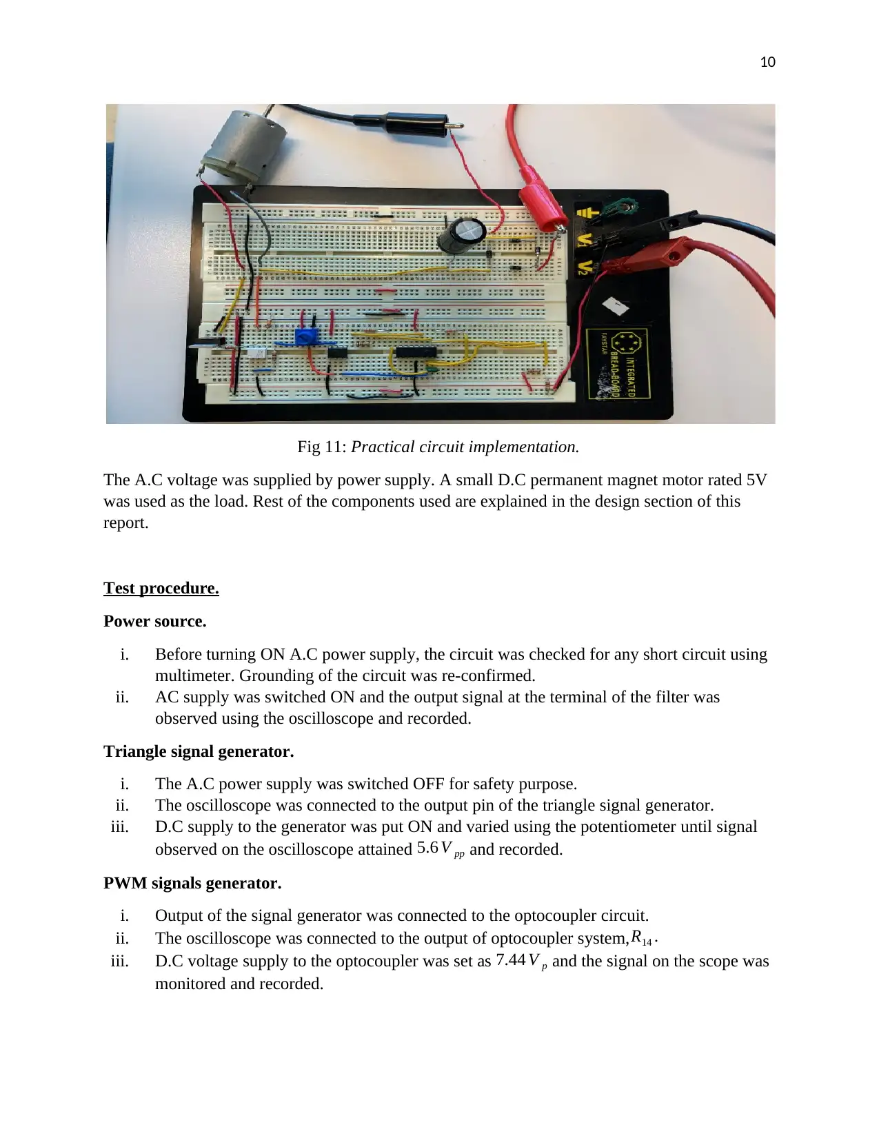
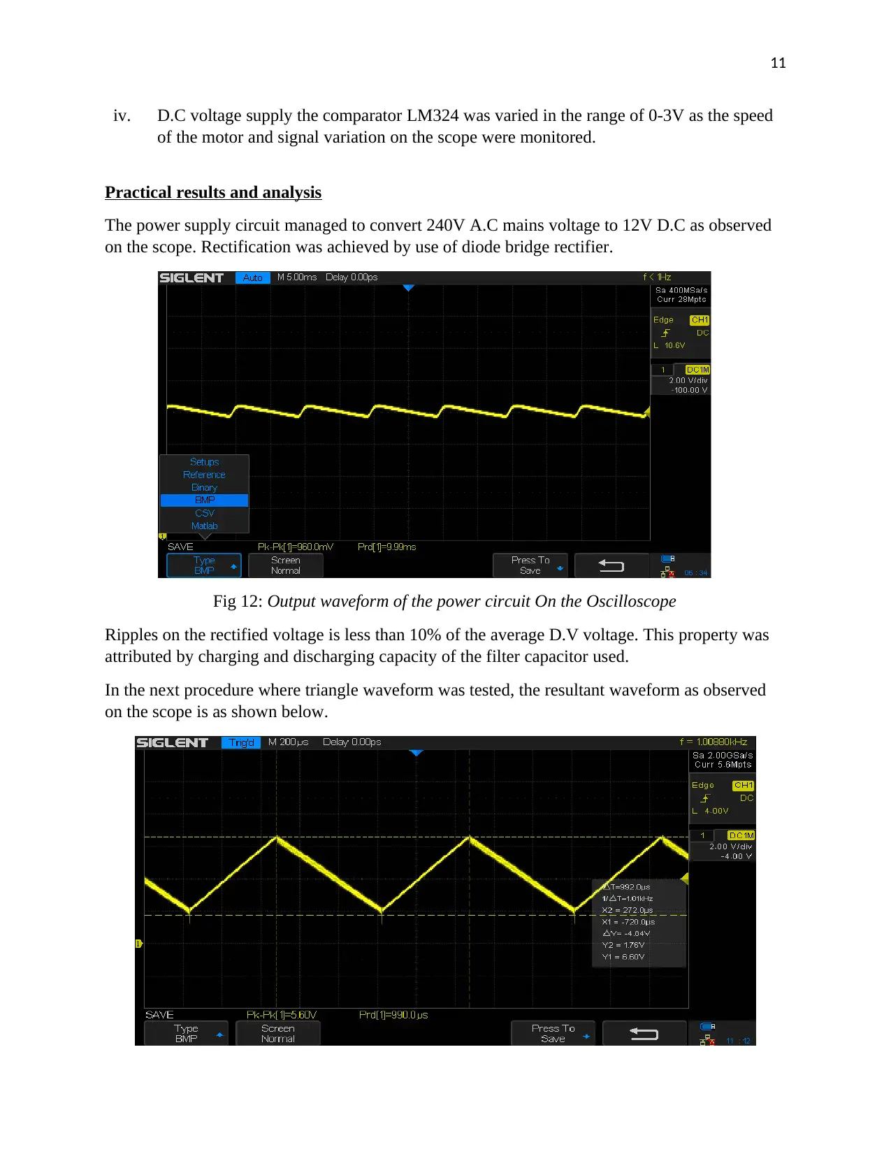
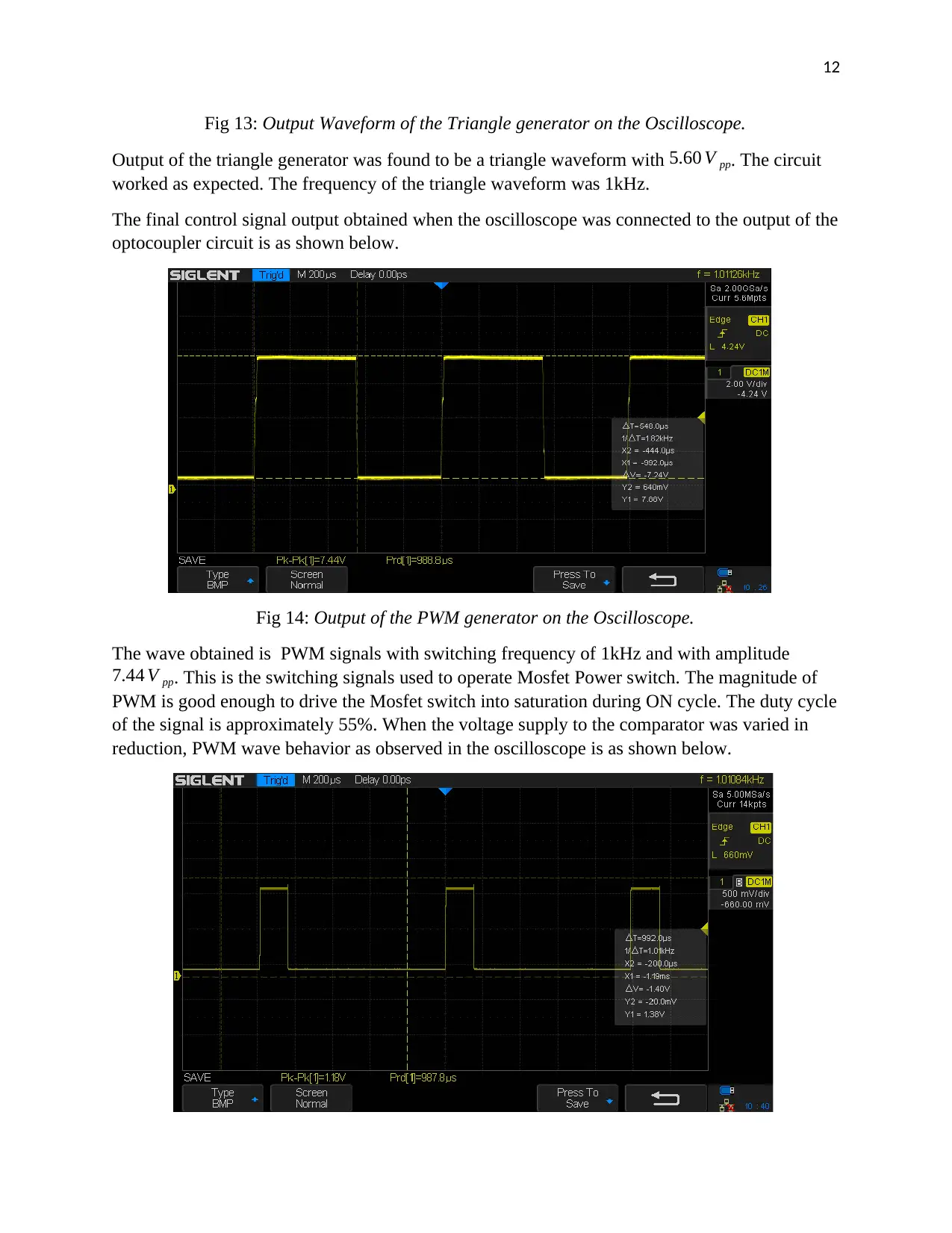
This report presents the design and implementation of a D.C motor speed control system using Pulse Width Modulation (PWM). The system converts AC power to DC, steps down the voltage, rectifies and filters it, and then uses a PWM signal to control the D.C motor's speed. The design includes a power supply converting 240V AC to a lower D.C voltage, a 1kHz triangle wave generator using an LM324 chip, and a PWM generator based on an LM311 voltage comparator. The control circuit is optically isolated from the motor circuit using an optocoupler. Simulations are performed using Circuit Lab Software to verify the design, and practical implementation is carried out on a breadboard with a small D.C permanent magnet motor. Test procedures and results are documented, showing the successful conversion of A.C to D.C, the generation of triangle waveforms, and the creation of PWM signals with varying duty cycles to control the motor speed.
Contribute Materials
Your contribution can guide someone’s learning journey. Share your
documents today.
1
Student
Instructor
Speed Control of D.C Motor
Date
Student
Instructor
Speed Control of D.C Motor
Date
Secure Best Marks with AI Grader
Need help grading? Try our AI Grader for instant feedback on your assignments.
2
Introduction
A D.C motor is a rotary electrical device that converts D.C electrical power into rotational
mechanical power. There are different types of D.C motors defined by the type and connection
of magnetic excitation circuit network. These types include series motors, shunt motors,
separately excited D.C motor, D.C permanent magnet motors etc. Thevenin’s equivalent circuit
of D.C motor is as shown below[1].
Fig 1: Thevenin’s equivalent circuit of separately excited D.C motor
The general voltage loop equation governing D.C motor can be derived from the above figure as
shown below.
V a =EA + Ia Ra (1)
But back e.m.f, EA can also be represented by
Ea =k ∅ ω (2)
Replacing equation 2 into equation 1, the resultant expression becomes
V a =k ∅ ω +I a Ra (3)
Rearranging equation 3 algebraically
ω= {V a }
{ k ∅ } − {Ra Ia }
{ k ∅ } (4)
From equation 4, it is clearly evidenced that angular speed of the motor is directly proportional
to the voltage supplied. Therefore, speed control of D.C motor is achieved by adjusting terminal
voltage supplied to the motor.
As aforementioned, D.C motor is supplied by D.C voltages for operation. However, most readily
available power supply is in A.C form. For the motor to be powered, it need to be interfaced with
a voltage converter system. Output of the voltage supply seemingly tends to be constant so long
as the A.C supply from power utility is constant. Speed control of the motor is then achieved by
varying output of the converter system. Variation of D.V voltage can be implemented in different
versions. For instance, small voltages can be adjusted using variable potentiometer. Systems with
relatively higher voltage, variation can be achieved by using Pulse Width Modulation (PWM)
system.
Detailed circuit Design.
3
The block diagram below represents the PWM DC motor control system whose speed is
variable.
Fig 2: Block diagram of D.C motor speed control.
The initial voltage supply to the motor system is in A.C form. A.C voltage is stepped down to
using the step-down transformer. Stepped down voltage is fed into the rectifier which outputs
D.V voltage. Rectified voltage is filtered to remove voltage ripples before being send into the
drive circuit. In the drive circuit, rectified and filtered voltage is modulated by PWM signals with
varying duty cycles (%D).
Designing of the D.C power supply.
The power supply is meant to convert 240V, 50Hz AC power supply to suitable low voltage for
rectifier bridge diodes.
Fig 3: Block diagram of Power supply.
It consists of the step-down transformer, bridge rectifier and filtering capacitor. The output
voltage of the bridge rectifier should not exceed 9V. By using the formula below, required
stepped down A.C voltage of the transformer is [2];
V ac= π
2 ( V d . c ) (5)
V ac= π
2 ( 12V )=18.8 V ac
Therefore, the secondary voltage of the transformer should be approximately 18.8 V ac at 50Hz.
The output voltage of the A.C supply was set to 18.8V.
The bridge rectifier was designed using 1N4001 diodes. These types of diodes have a current
carrying capacity of 1A and can withstand current peaks up to 30 A as well as block peak
4
reverse voltage of 50 V. Reverse leakage current for these diodes is 5 μA. With our D.C motor as
the load, this type of diodes was the most preferred.
Voltage ripples in the D.C output voltage waveform of the full-wave bridge rectifier is
suppressed by filtering capacitor. The capacitance value for this application was calculated as
follow.
CF = { ¿ }
V (6)
Where CF is the capacitance value , I i s the load current , ( t ) i s half cycle time and V is the
maximum ripple of the rectified voltage. Current rating of the D.C motor is 0.5A and A.C mains
voltage frequency is 50Hz. Therefore,
t=0.5 × 1
50 Hz =0.01 sec (7)
Substituting equation 7 into equation 6
CF = { 0.5× 0.01 sec }
9V =0.0011 F=1111 μF
The suitable capacitor rating found for the application is rated 220 μF 25 V .
Designing of a 1kHz triangle wave generator with supply of 9 V.
In this stage, the design of triangle wave generator was based on LM324 chip. The cheap has
quadruple operation amplifiers. The single supply range voltage for each op amp is 3V to 32V.
The switching square wave that is provided by non-inverting Schmitt rigger is 4.5V. Suppose the
peak of triangle waveform is 3.6V, then resistor R3∧R4 were computed as shown below.
Secure Best Marks with AI Grader
Need help grading? Try our AI Grader for instant feedback on your assignments.
5
Fig 4: Triangle generator wave circuit in CircuitLab Software.
V triangle=4.5V × R4
R3
=3.6V (8)
Rearranging equation (8) algebraically, the resultant becomes;
R4
R3
= 3.6
4.5 (9)
Thus, by selecting R3=10 kΩ, then R4 =8 kΩ
The ramp of triangle waveform falls at a steady state rate, which can be defined by the equation
below.
Ramp= {−V triangle }
{R7 C } = {−V triangle }
{ ∆ t } (10)
Where R7 C is capacitor time constant. Capacitor time constant is the duration required for
capacitor to discharge 63% of its charge on the negative gradient of the ramp. In one cycle,
equation 10 becomes;
Ramp=4 {−V triangle }
{ R7 C } =4 {−V triangle }
{ ∆ t } (11)
Since the desired frequency of the triangle wave is 1kHz, then { ∆ t } can be computed as;
{ ∆ t }= {R7 C }= 1
1000 Hz =0.001 sec (12)
6
Selecting R7 =28 kΩ, then C was computed by substituting R7 in equation (12)
C= 0.001
28000 =35.71nF (13)
The capacitance value available however, is 10 nF.
Non-inverting Schmitt trigger and integrator are supplied by 4.5 V from 9V source.
Using voltage divider rule, resistors R5∧R6 were determined as shown in the expression below.
4.5 V = R6
{ R5+ R6 } × 9 V
Setting R5=22kΩ and replacing in equation 14, then R6 =22 kΩ.
Designing PWM generator.
The PWM generator design was based on the triangle output waveform of the triangle wave
generator and LM311 voltage comparator.
The comparator works by comparing triangle waveform fed to the negative terminal and the D.C
voltage fed to the positive terminal. The resultant output waveform of the comparator is PWM.
Fig 5: Optocoupler circuit in CircuitLab Software.
7
Duty cycles of the PWM is varied by adjusting D.C voltage using a 10 kΩ potentiometer supplied
by 9V D.C. The control circuit system consisting of the triangle wave generator and PWM
generator is optically isolated from the motor circuit using 4N25 optocoupler. Main functions of
optocoupler are to isolate low voltage control circuit from relatively high voltage motor circuit
and to amplify PWM signal to switching voltage of magnitude 10 V that is enough to operate
IRF530 Mosfet switch. Pull down resistor of the optocoupler circuit was chosen as R15=240 Ω
while current limiting resistance was selected to be R14=120Ω.
Mosfet switch is used to vary D.V voltage supplied to the motor by varying duty cycles between
0% to 100%. Negative terminal of the motor is connected to the drain terminal while source
terminal is grounded. Optocoupler output is connected to the gate terminal via a current limiting
resistor R14. Grounding of the motor circuit is completely isolated from the grounding of control
circuit so as to enable optcoupler operate as expected. Common grounding shorts the
optocoupler.
The complete design circuit is as shown below
Fig 6
Simulations of the design.
The power supply was constructed in Circuit Lab Software as shown below.
Paraphrase This Document
Need a fresh take? Get an instant paraphrase of this document with our AI Paraphraser
8
Fig 7: Power supply circuit in CircuitLab Software.
Secondary voltage of the transformer and voltage across filter capacitor C1 and load resistor R1
were observed using virtual oscilloscope as shown below.
Stepped down A.C voltage Rectified voltage
Fig 8: Output signals of power supply in CircuitLab Software.
240V, 50Hz primary voltage was stepped down to 12V, 50Hz secondary voltage. The voltage
across filter capacitor C1 and load resistor R1 was a 12V D.C voltage characterized by small
suppressed ripples.
9
The triangle wave generator in fig 4 was as well constructed in Circuit Lab Software. The
resultant output waveforms obtained is as shown below.
Fig 9: Output of the triangle generator in Circuit Lab Software.
The triangle waveform of 8.5 V p was realized as the output of the triangle wave generator.
Switching frequency of the triangle wave was found to be 1kHz.
Optocoupler circuit was then connected to the output of the triangle wave generator. Using
virtual oscilloscope in Circuit Lab Software, the wave observed at the output terminal of the
optocoupler circuit was as shown below.
Fig 10: PWM wave of the PMW generator output in CircuitLab Software.
The wave is a PWM type with peak voltage of 8.5 V and 1kHz switching frequency.
Practical implementation
The circuit in fig 6 was constructed on the breadboard as shown below.
10
Fig 11: Practical circuit implementation.
The A.C voltage was supplied by power supply. A small D.C permanent magnet motor rated 5V
was used as the load. Rest of the components used are explained in the design section of this
report.
Test procedure.
Power source.
i. Before turning ON A.C power supply, the circuit was checked for any short circuit using
multimeter. Grounding of the circuit was re-confirmed.
ii. AC supply was switched ON and the output signal at the terminal of the filter was
observed using the oscilloscope and recorded.
Triangle signal generator.
i. The A.C power supply was switched OFF for safety purpose.
ii. The oscilloscope was connected to the output pin of the triangle signal generator.
iii. D.C supply to the generator was put ON and varied using the potentiometer until signal
observed on the oscilloscope attained 5.6 V pp and recorded.
PWM signals generator.
i. Output of the signal generator was connected to the optocoupler circuit.
ii. The oscilloscope was connected to the output of optocoupler system, R14 .
iii. D.C voltage supply to the optocoupler was set as 7.44 V p and the signal on the scope was
monitored and recorded.
Secure Best Marks with AI Grader
Need help grading? Try our AI Grader for instant feedback on your assignments.
11
iv. D.C voltage supply the comparator LM324 was varied in the range of 0-3V as the speed
of the motor and signal variation on the scope were monitored.
Practical results and analysis
The power supply circuit managed to convert 240V A.C mains voltage to 12V D.C as observed
on the scope. Rectification was achieved by use of diode bridge rectifier.
Fig 12: Output waveform of the power circuit On the Oscilloscope
Ripples on the rectified voltage is less than 10% of the average D.V voltage. This property was
attributed by charging and discharging capacity of the filter capacitor used.
In the next procedure where triangle waveform was tested, the resultant waveform as observed
on the scope is as shown below.
12
Fig 13: Output Waveform of the Triangle generator on the Oscilloscope.
Output of the triangle generator was found to be a triangle waveform with 5.60 V pp. The circuit
worked as expected. The frequency of the triangle waveform was 1kHz.
The final control signal output obtained when the oscilloscope was connected to the output of the
optocoupler circuit is as shown below.
Fig 14: Output of the PWM generator on the Oscilloscope.
The wave obtained is PWM signals with switching frequency of 1kHz and with amplitude
7.44 V pp. This is the switching signals used to operate Mosfet Power switch. The magnitude of
PWM is good enough to drive the Mosfet switch into saturation during ON cycle. The duty cycle
of the signal is approximately 55%. When the voltage supply to the comparator was varied in
reduction, PWM wave behavior as observed in the oscilloscope is as shown below.
13
Fig 15: PWM with Varying duty cycles
It can be clearly seen that Duty cycle of PWM signals has reduced with reduction in control
voltage of the comparator. Duty cycle is approximately 20%. Also, there was a relative speed
reduction when duty cycle was reduced from 55% to 20%. According to equation 4, velocity of
the motor is directly proportional to the supplied voltage. Therefore, as there is reduction in duty
cycle, voltage supplied to the motor is correspondingly reduced. As a result, speed reduction is
realized. Concurrently, an increase in duty cycle increases voltage supplied to the motor, hence
increase in speed.
Paraphrase This Document
Need a fresh take? Get an instant paraphrase of this document with our AI Paraphraser
14
REFERENCES
[1] S. J. Chapman, ELECTRIC MACHINERY FUNDAMENTALS, BAE SYSTEMS Australia:
McGraw-Hill, 2005.
[2] A. H. A. B. DRURY, ELECTRIC MOTORS DRIVES fundamentals, types, and application,
The Boulevard, Langford Lane, Kidlington, Oxford, : Elsevier, Fourth edition 2013.
BILL OF QUANTITIES
Number Component Quantity Price each
in USD
Total cost
in USD
Manufacturer
1 1N4001 Diodes 4 0.02 0.08 New Jersey
Semiconductor
Product Inc
2 Electrolytic
(220uF 25V and
( 0.5uF 20V)
2 0.05 0.10 Nuintek
Co.LTD
3 LM324 Chip 1 0.08 0.08 Intersil
Corporation
4 LM311 Chip 1 0.06 0.06 NXP
5 IRF530 Mosfet 1 0.90 0.09 Intersil
Corporation
6 4N25 Optocoupler 1 0.04 0.04 Toshiba
Semiconductors
7 10kΩ
Potentiometer
1 0.01 0.01
8 Resistors (2(10kΩ)
8 kΩ, 2(22 kΩ)
26.8 kΩ, 100 Ω
120 Ω, 240 Ω)
9 0.01 0.09
9 Integrated Bread
Board
1 3.00 3.00
10 5V permanent 1 0.50 0.50
15
magnet D.C motor
11 Connecting wires 1 0.09 0.09 Shenzhen
Kinmore Motor
Co.Ltd
TOTAL $.4.14
magnet D.C motor
11 Connecting wires 1 0.09 0.09 Shenzhen
Kinmore Motor
Co.Ltd
TOTAL $.4.14
1 out of 15
Your All-in-One AI-Powered Toolkit for Academic Success.
+13062052269
info@desklib.com
Available 24*7 on WhatsApp / Email
Unlock your academic potential
© 2024 | Zucol Services PVT LTD | All rights reserved.