Analogue Analysis and Design (ENG530) Filter Portfolio: 2018/19

Verified

Added on  2022/07/29

|17
|1493
|31
Practical Assignment
AI Summary
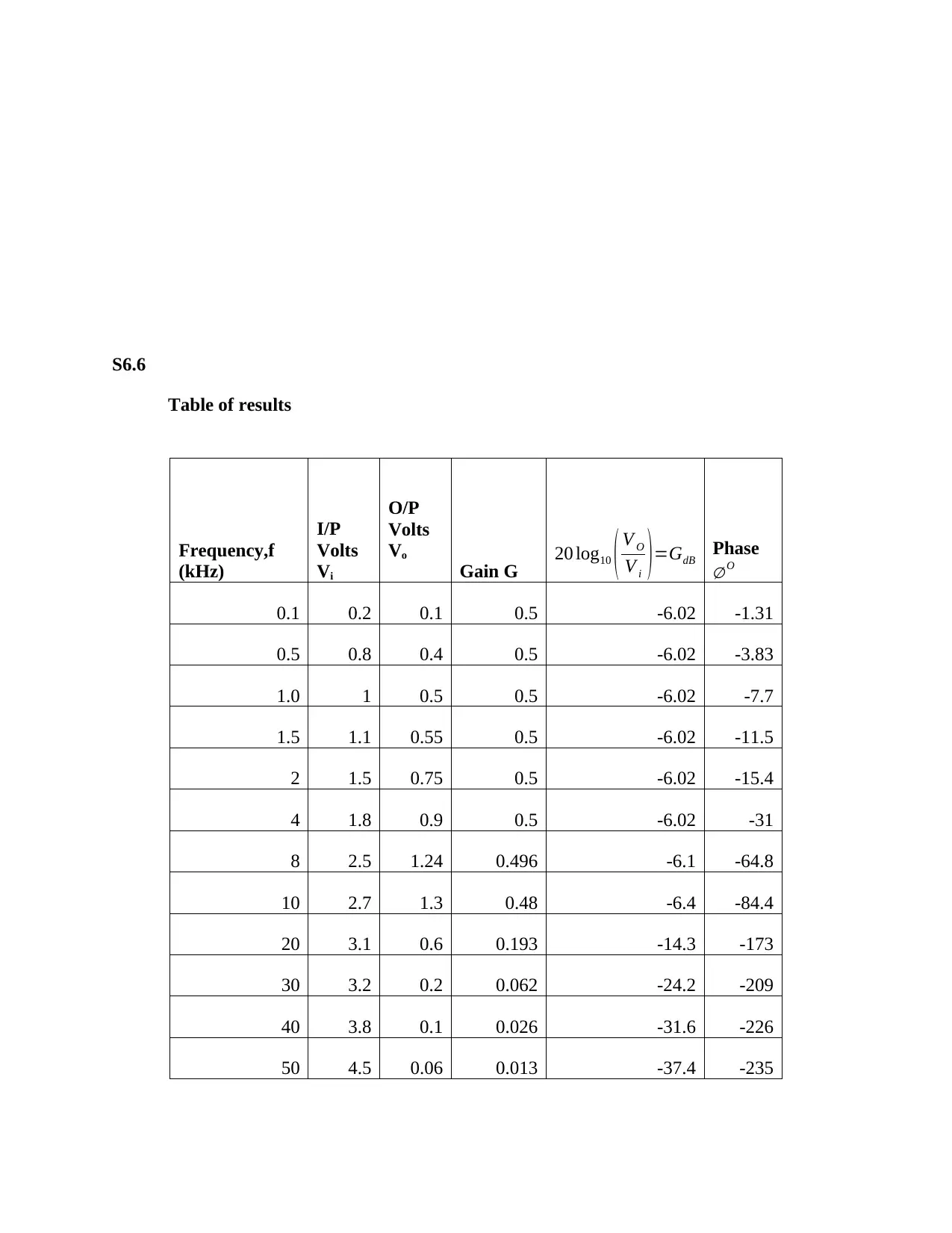
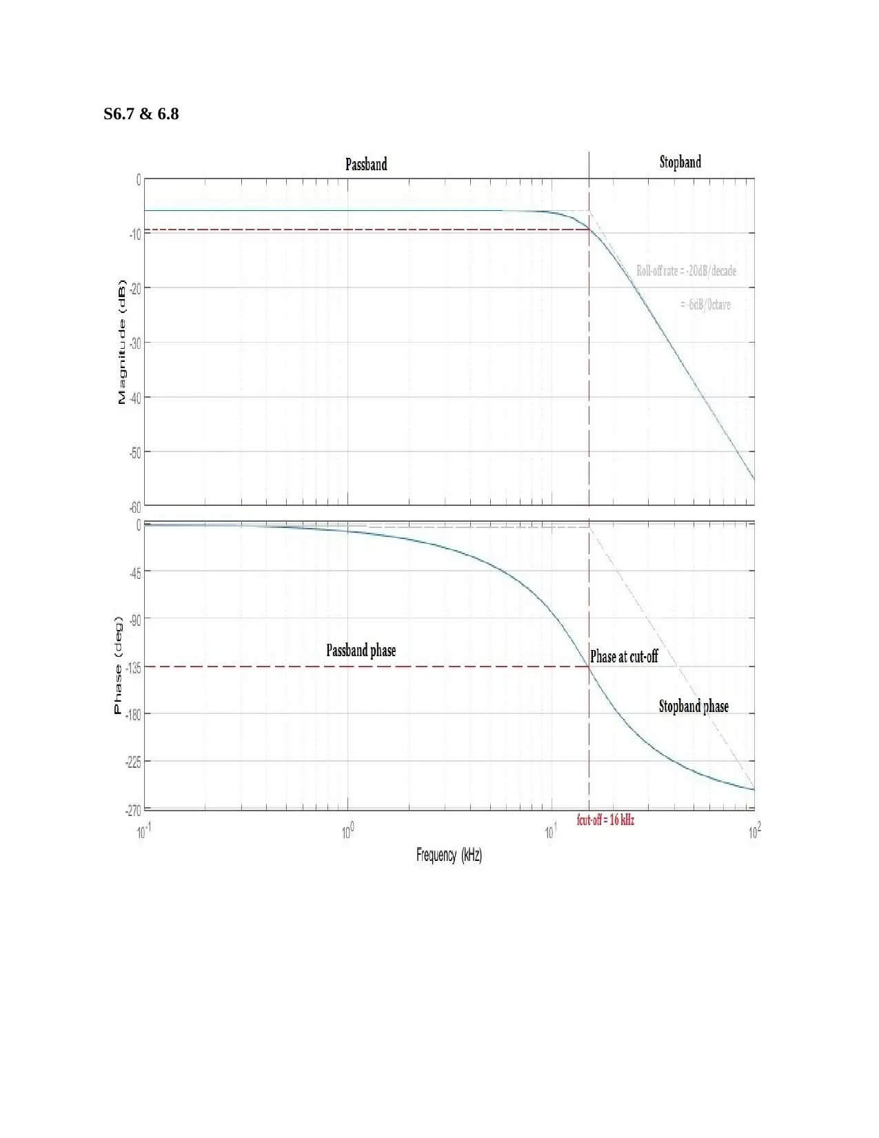
This document presents a comprehensive portfolio on analogue filter design and analysis, specifically focusing on RC and LC low-pass filters. The assignment requires students to design, build, and analyze these filters, including the derivation of transfer functions and two-port network representations using Z-parameters. The analysis involves calculating cutoff frequencies, gain, and phase characteristics, comparing theoretical values with experimental results obtained through circuit simulation and physical implementation. The portfolio also addresses the impact of component tolerances and provides insights into the observed discrepancies between theoretical and practical outcomes, along with relevant references. The assignment emphasizes the practical application of theoretical knowledge in analogue electronics, aligning with the ENG530 course curriculum.
Document Page
S5.1 Circuit Diagram
S5.2
Output impedance of the function generator, RS = 50Ω
Input impedance of the oscilloscope, RL = 1
S5.3
Cut off frequency, fc = 10 kHz
S5.4
The cut-off frequency of the filter in question is 10 kHz and is given by the equation
f c= 1
2 π Req C
Req takes into account both the source and load resistance. If the value of capacitance (C) is
chosen to be C=0.01 μF, the resistance is approximately
Req = 1
2 π f c C 1.591 k Ω
Thus,
Capacitor, C =0.33 F
Resistance, R 1.591
tabler-icon-diamond-filled.svg

Paraphrase This Document

Need a fresh take? Get an instant paraphrase of this document with our AI Paraphraser
Document Page
S5.5
Find an attached file of the RC circuit as built in multism
S5.6
The preferred standard manufactured values for the capacitor and the resistor are:
Capacitor, C = (10 + 000 +/- 5%) pF = 0.015 % μ F
Resistance, R 16 x 102 5 % Ω=1.6 5 %k Ω
S5.7
Frequency,f
(kHz)
I/P
Volts
Vi
O/P Volts
Vo
Gain G 20 log10 ( V O
V i ) =GdB Phase
O
0.1 0.2 0.2 1 0 -0.85
0.5 0.8 0.8 1 0 -2.97
0.8 1 1 1 0 -4.74
1 1.1 1.1 1 0 -5.94
2 1.5 1.5 1 0 -11.7
4 1.8 1.66 0.9222 -0.70329 -22.5
6 2.2 1.87 0.85 -1.41162 -31.9
8 2.4 1.84 0.7667 -2.30787 -39.6
10 3 2.08 0.6933 -3.18116 -46
20 3.2 1.39 0.4344 -7.2427 -64.2
40 4 0.94 0.235 -12.5786 -76.4
50 4.5 0.85 0.1889 -14.4759 -79
90 5 0.54 0.108 -19.3315 -83.9
Document Page
S5.8 & S5.9
Document Page
S5.10 Graph Measurements:
S5.10.1 The cut-off frequency is 10 kHz (as indicated on the graphical plots)
f c
actual=10 kHz
S5.10.2 The per decade slope of the gain magnitude is -20dB/decade (as indicated on the
graphical plots)
Sactual
decade =20 dB /decade
S5.10.3 The per octave slope of the gain magnitude is -6dB/octave (as indicated on the graphical
plots)
Sactual
octave =6 dB /octave
S5.10.4 The pass band phase is between 0 to -45o (as indicated on the graphical plots). In
radians,
1
4 π θactual
pass 0
S5.10.5 The stop band phase is between -45o to -90o (as indicated on the graphical plots). In
radians,
π
2 θactual
stop 1
4 π
S5.10.6 The phase in radians at the cut-off frequency is obtained from the graph as -45o. In
radians,
θactual
cutoff =45
180 π =1
4 π rads
S5.10.7 The cut-off frequency obtained from the graph is 10 kHz and that in design specification
is 10 kHz. Therefore the fractional difference is zero i.e.
Ef =0
tabler-icon-diamond-filled.svg

Paraphrase This Document

Need a fresh take? Get an instant paraphrase of this document with our AI Paraphraser
Document Page
S5.11 Derivation of the transfer function for the filter circuit
From the equivalent circuit diagram in S.5.1, the transfer function is derived as below
The output voltage is obtained by voltage divider rule as,
V out =
( RL
sC
RL + 1
sC )
(Rs + R+
RL
sC
RL+ 1
sC ) V ¿
Simplifying the expression,
V out =
( RL
1+sC RL )
( Rs + R+ RL
1+ sC RL ) V ¿
On re-arranging, the transfer function for the above filter reduces to,
V out
V ¿
= RL
Rs + R+RL+ sC RL( Rs + R)
But the output impedance of the function generator, RS = 50Ω and the input impedance of the
oscilloscope, RL = 1 . Substituting these values in the above expression, the transfer function
becomes,
V out
V ¿
= (1 x 10⁶)
50+ R+(1 x 10⁶ )+(1 x 10⁶)sC (50+ R)
The calculated values of the capacitor (C) and the resistor (R) at the cut-off frequency are 0.01
μ F and 1.6 k Ω respectively. Replacing these values in the transfer function above, the equation
reduces to
H ( s )= V out
V ¿
= 106
1001650+ 16.5 s
Document Page
The above transfer function is in the s-domain. To convert it the complex frequency domain, s is
replaced with . The result is
H ( ) = V out
V ¿
= 106
1001650+ j 16.5 ω
S5.12 Derivation of the two port representation of the circuit
The two port network is defined in terms of Z-parameters. For the given RC network, the Z-
parameters are obtained as follows:
Z11= V 1
I1 |(I ¿¿ 2=0)=Rs + R+ 1
jωC ¿
Z21= V 2
I 1 |( I¿¿ 2=0)= 1
jωC ¿
Z22= V 2
I2 |(I ¿¿ 1=0)= 1
jωC ¿
Z12= V 1
I 2 |(I ¿¿ 1=0)= 1
jωC ¿
For C=0.33 FR=1.591 , Rs=50 Ω
Z11=1.591 x 10³ +50+ 1
j 2 π x 10 x 0.33 x 103 =1641 j 4.82 x 10⁵ Ω
Z12= 1
j 2 π x 10 x 0.33 x 103 = j 4.82 x 10⁵ Ω
Z22= 1
j 2 π x 10 x 0.33 x 103 = j 4.82 x 10⁵ Ω
Z21= 1
j 2 π x 10 x 0.33 x 103 = j 4.82 x 10⁵ Ω
In matrix form, it is
[ Z ]= [ 1641 j 4.82 x 10⁵ j 4.82 x 10⁵
j 4.82 x 10⁵ j 4.82 x 10⁵ ]
Document Page
6. Passive LC Low Pass Filter
S6.1
S6.2
Cut-off frequency, fc = 15 kHz
S6.3
Component values of the components are obtained from the defining equations of the filter. The
cut-off frequency is given by the relation,
ωc= 2
LC rad s1
In hertz, the frequency is
tabler-icon-diamond-filled.svg

Paraphrase This Document

Need a fresh take? Get an instant paraphrase of this document with our AI Paraphraser
Document Page
f c= 1
π LC
If a capacitor value of 0.1 μ F is chosen, the inductor value is
L= ( 1
π f c C )2
4.503 mH
The matching impedances Rs and RL are therefore obtained as
Rs=RL= L
C 212.21 Ω
Inductor, L = 4.503 mH
Capacitor, C = 0.1 μ F
S6.4
Find an attached file of the LC circuit as built in multism
S6.5
The standard preferred manufacturer’s values are;
L = (45 + 00 +/- 1%) μ H = 4.5 mH
C = (10 + 0000 +/- 5%) pF = 0.1 5 % μ F
Document Page
S6.6
Table of results
Frequency,f
(kHz)
I/P
Volts
Vi
O/P
Volts
Vo
Gain G 20 log10 ( V O
V i ) =GdB Phase
O
0.1 0.2 0.1 0.5 -6.02 -1.31
0.5 0.8 0.4 0.5 -6.02 -3.83
1.0 1 0.5 0.5 -6.02 -7.7
1.5 1.1 0.55 0.5 -6.02 -11.5
2 1.5 0.75 0.5 -6.02 -15.4
4 1.8 0.9 0.5 -6.02 -31
8 2.5 1.24 0.496 -6.1 -64.8
10 2.7 1.3 0.48 -6.4 -84.4
20 3.1 0.6 0.193 -14.3 -173
30 3.2 0.2 0.062 -24.2 -209
40 3.8 0.1 0.026 -31.6 -226
50 4.5 0.06 0.013 -37.4 -235
Document Page
90 13 0.03 0.0023 -52.7 -251
tabler-icon-diamond-filled.svg

Paraphrase This Document

Need a fresh take? Get an instant paraphrase of this document with our AI Paraphraser
Document Page
S6.7 & 6.8
Document Page
S6.9 Graph Measurements:
S6.9.1 The cut-off frequency is 10 kHz (as indicated on the graphical plots)
f c
actual=16 kHz
S6.9.2 The per decade slope of the gain magnitude is -20dB/decade (as indicated on the
graphical plots)
Sactual
decade =20 dB /decade
S6.9.3 The per octave slope of the gain magnitude is -6dB/octave (as indicated on the graphical
plots)
Sactual
octave =6 dB /octave
S6.9.4 The pass band phase is between 0 to -135o i.e. angles greater than -135 degrees (as
indicated on the graphical plots). In radians,
3
4 π θactual
pass 0
S6.9.5 The stop band phase is between -135o to -360o i.e. angles less than 135 degrees (as
indicated on the graphical plots)
2 π θactual
stop 3
4 π
S6.9.6 The phase in radians at the cut-off frequency is obtained from the graph as
θactual
cutoff =135
180 π=3
4 π rads
S6.9.7 The cut-off frequency obtained from the graph is 16 kHz and that in design specification
is 15 kHz. Therefore the fractional difference is
¿ |1615|
15 ×100 ¿ 6.6667 %
Ef =6.6667 %
chevron_up_icon
1 out of 17
circle_padding
hide_on_mobile
zoom_out_icon
[object Object]