A Review on CMOS-Compatible Spintronic Devices and Applications
VerifiedAdded on 2022/09/14
|11
|6747
|12
Report
AI Summary
This paper provides a comprehensive review of CMOS-compatible spintronic devices, exploring their potential to overcome the limitations of traditional CMOS technology. The review begins with an introduction to spintronics, including the principles of magnetoresistance and spin-transfer torque, and then delves into the application of these principles in memory devices, such as magnetoresistive random-access memory (MRAM). The paper discusses various aspects of spintronic memory, including free layer design, spin-transfer torque memory, and magnetoelectric effects. It also examines the physics behind key spintronic phenomena like giant magnetoresistance and tunnel magnetoresistance, and how these effects are utilized in spintronic devices. The review highlights the advancements in spintronic memory technologies, comparing spin transfer torque-magnetoresistive random-access memory, spin-orbit torque magnetoresistive random-access memory, and domain wall motion magnetoresistive random-access memory. The paper concludes by emphasizing the importance of spintronics in the development of future low-power, high-performance integrated circuits.
1Abstract— CMOS have successfully been scaled down for
numerous decades to attain not only nuanced performance but
also increased speed of integrated circuits is more affordable
costs. Charge-based CMOS of this generation face two key
challenges: variability and dissipation of power. Spintronics
is a fast evolving field of study besides development that
provides possible solution to such challenges via introduction
of novel more than Moore devices. Spin-based
magnetoresistive random-access memory is acknowledged
already one of most hopeful options for use in coming
universal memory. Magnetic tunnel junctions which are
major elements within magnetoresistive random-access
memory cells may as well be used in building logic-in-
memory circuits having non-volatile elements mounted at top
of CMOS logic circuits. This paper is a review of CMOS-
compatible spintronics uses where a short introduction to
physical background is presented followed by a thorough
review of state of art spintronics gadgets used in memory
applications. .
Keywords: spintronics, magnetoresistance, spin oscillator,
spin torque
I. INTRODUCTION
An increase in speed has been witnessed in search of a new
technology that is able to replace or even complement CMOS
as a result of rapid approach of CMOS miniaturization to
intrinsic limits. The principle of operation of MOSFET is
mainly pegged on degree of charge of freedom of electrons.
The electron spin which is another property of intrinsic
electron attracts a lot of attention at the moment as a portable
replacement for complementing charge freedom degree for
use in future devices [1]. Characterization of electron spin
state is done using one of two of possible projects on specific
1
Student Name (student number) is studying XXXX engineering in
Griffith School of Engineering and buildt Environment, Griffith University.
Email F.Author@griffithuni.edu.au
.
axis and is usable in digital processing of information. A
small amount of energy is needed to invert orientation of spin
which is needed for applications in regions that have low
power. The electron spin may be pointing in whichever
direction on single Bloch sphere and such feature is adopted
in quantum computing, nevertheless, successful adoption of
this computer based on spin quibits within silicon needs
cryogenic temperatures.
The relaxation time for spin for conducting electrons that
derives characteristic time for various non-equilibrium spin
relations in direction of its value of equilibrium lies in range
of nanoseconds at room temperature. Hence, length of
diffusion of spin lies within micrometer anger with spin
conducting electrons being usable in transferring, encoding or
even processing of information. In such a case, electron spin
degree of freedom is adopted in binary mode. Important to
note is that transfer of information of spin does not need a
flow in charge current. Such decoupling of sin form charge
renders spin degree of freedom a reliable option of low power
application.
Th proposal of complementing or total replacement of charge
degree of freedom by spin has been in place for more than
three decades, including an illustration of basic elements
needed for applications related to spin for instance spin-
polarized currents injection in silicon, manipulation and
detection of spin were not available until lately. In as much as
it appears direct injecting spin-polarized carriers inside
silicon from ferromagnetic contact, an integral conductivity
mismatch between silicon and a ferromagnetic contact
inhibits injection of spin [2].
A unique method based on hot electrons attenuation with
spins that are not parallel to magnetization of ferromagnetic
films enables creation of imbalance between electrons with
spin-down as well as spin-up within silicon hence injection of
spin-polarized current [13]. The spin-coherent movement via
device was researched via application of an external magnetic
field resulting in precession of spins at time of their
propagation to drain from source. The detection is done using
1
A REVIEW ON COMPATIBLE CMOS-SPINTRONIC DEVICESStudent Name and student number
Paraphrase This Document
Need a fresh take? Get an instant paraphrase of this document with our AI Paraphraser
similar hot electron spin filter with set-up of experiment
representing first two terminal silicon devices driven by spin
that may be anticipated operating at room temperature. This
paper presents a review of CMOS-compatible spintronics
applications and begins by a summary review on spintronics
background and thereafter a review of recent progress
alongside discussion on current state of art of spintronics
applications in logic, memory, oscillations among other
applications.
II. BASICS OF SPINTRONICS
Magnetoresistance
The giant magnetoresistance alongside tunnel
magnetoresistance effects are among leading impressive
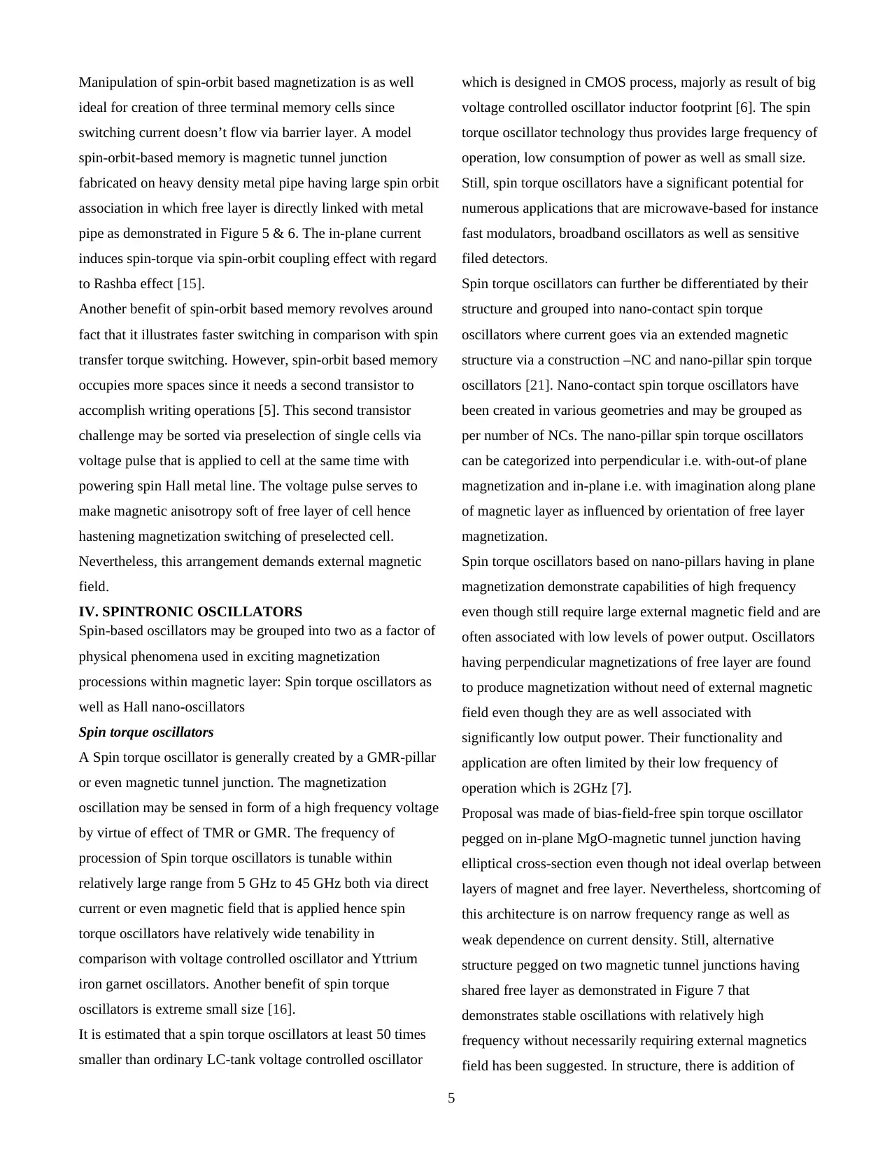
outcomes of spin spintronics. Giant magnetoresistance have
been observed in Fe/Cr super lattices where giant
magnetoresistance is sensed within pillar composed of not
less than two ferromagnetic layers separated from each other
by a spacer layer that is non-magnetic [19]. The pillar
resistance is factor of direction of magnetization of layer in
relation to each other.
The giant magnetoresistance source as demonstrated in
Figure 1 defines equivalent scattering of two categories of
electrons with various orientations of spin in relation to
direction of magnetization of layers are same, spin-down
electrons are able to propagate and pass via structure almost
unscattered leading to high electron conductivity and thus
low resistance[3]. On other hand, in anti-parallel state there is
collision of both spin-up and spin-down within ferromagnetic
layers resulting in high resistance.
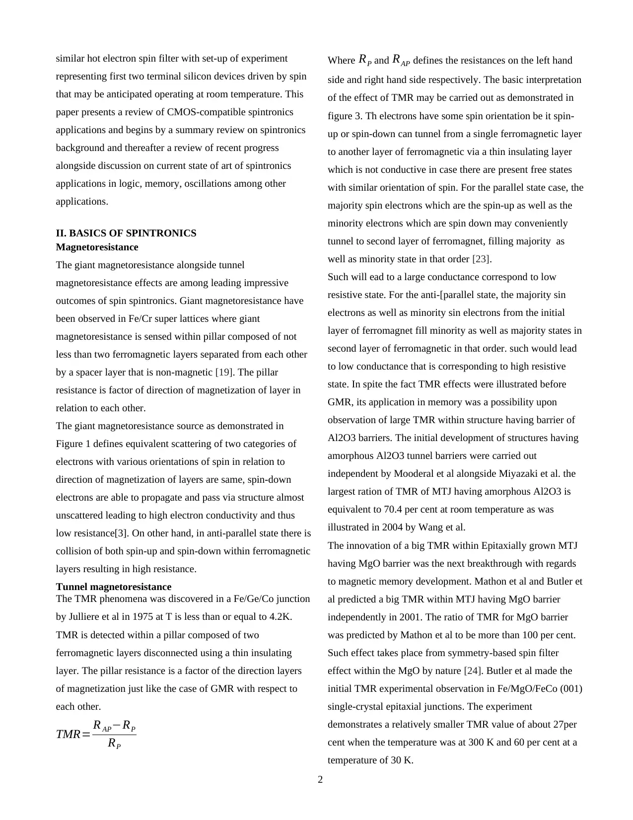
Tunnel magnetoresistance
The TMR phenomena was discovered in a Fe/Ge/Co junction
by Julliere et al in 1975 at T is less than or equal to 4.2K.
TMR is detected within a pillar composed of two
ferromagnetic layers disconnected using a thin insulating
layer. The pillar resistance is a factor of the direction layers
of magnetization just like the case of GMR with respect to
each other.
TMR= R AP−RP
RP
Where RP and RAP defines the resistances on the left hand
side and right hand side respectively. The basic interpretation
of the effect of TMR may be carried out as demonstrated in
figure 3. Th electrons have some spin orientation be it spin-
up or spin-down can tunnel from a single ferromagnetic layer
to another layer of ferromagnetic via a thin insulating layer
which is not conductive in case there are present free states
with similar orientation of spin. For the parallel state case, the
majority spin electrons which are the spin-up as well as the
minority electrons which are spin down may conveniently
tunnel to second layer of ferromagnet, filling majority as
well as minority state in that order [23].
Such will ead to a large conductance correspond to low
resistive state. For the anti-[parallel state, the majority sin
electrons as well as minority sin electrons from the initial
layer of ferromagnet fill minority as well as majority states in
second layer of ferromagnetic in that order. such would lead
to low conductance that is corresponding to high resistive
state. In spite the fact TMR effects were illustrated before
GMR, its application in memory was a possibility upon
observation of large TMR within structure having barrier of
Al2O3 barriers. The initial development of structures having
amorphous Al2O3 tunnel barriers were carried out
independent by Mooderal et al alongside Miyazaki et al. the
largest ration of TMR of MTJ having amorphous Al2O3 is
equivalent to 70.4 per cent at room temperature as was
illustrated in 2004 by Wang et al.
The innovation of a big TMR within Epitaxially grown MTJ
having MgO barrier was the next breakthrough with regards
to magnetic memory development. Mathon et al and Butler et
al predicted a big TMR within MTJ having MgO barrier
independently in 2001. The ratio of TMR for MgO barrier
was predicted by Mathon et al to be more than 100 per cent.
Such effect takes place from symmetry-based spin filter
effect within the MgO by nature [24]. Butler et al made the
initial TMR experimental observation in Fe/MgO/FeCo (001)
single-crystal epitaxial junctions. The experiment
demonstrates a relatively smaller TMR value of about 27per
cent when the temperature was at 300 K and 60 per cent at a
temperature of 30 K.
2
representing first two terminal silicon devices driven by spin
that may be anticipated operating at room temperature. This
paper presents a review of CMOS-compatible spintronics
applications and begins by a summary review on spintronics
background and thereafter a review of recent progress
alongside discussion on current state of art of spintronics
applications in logic, memory, oscillations among other
applications.
II. BASICS OF SPINTRONICS
Magnetoresistance
The giant magnetoresistance alongside tunnel
magnetoresistance effects are among leading impressive
outcomes of spin spintronics. Giant magnetoresistance have
been observed in Fe/Cr super lattices where giant
magnetoresistance is sensed within pillar composed of not
less than two ferromagnetic layers separated from each other
by a spacer layer that is non-magnetic [19]. The pillar
resistance is factor of direction of magnetization of layer in
relation to each other.
The giant magnetoresistance source as demonstrated in
Figure 1 defines equivalent scattering of two categories of
electrons with various orientations of spin in relation to
direction of magnetization of layers are same, spin-down
electrons are able to propagate and pass via structure almost
unscattered leading to high electron conductivity and thus
low resistance[3]. On other hand, in anti-parallel state there is
collision of both spin-up and spin-down within ferromagnetic
layers resulting in high resistance.
Tunnel magnetoresistance
The TMR phenomena was discovered in a Fe/Ge/Co junction
by Julliere et al in 1975 at T is less than or equal to 4.2K.
TMR is detected within a pillar composed of two
ferromagnetic layers disconnected using a thin insulating
layer. The pillar resistance is a factor of the direction layers
of magnetization just like the case of GMR with respect to
each other.
TMR= R AP−RP
RP
Where RP and RAP defines the resistances on the left hand
side and right hand side respectively. The basic interpretation
of the effect of TMR may be carried out as demonstrated in
figure 3. Th electrons have some spin orientation be it spin-
up or spin-down can tunnel from a single ferromagnetic layer
to another layer of ferromagnetic via a thin insulating layer
which is not conductive in case there are present free states
with similar orientation of spin. For the parallel state case, the
majority spin electrons which are the spin-up as well as the
minority electrons which are spin down may conveniently
tunnel to second layer of ferromagnet, filling majority as
well as minority state in that order [23].
Such will ead to a large conductance correspond to low
resistive state. For the anti-[parallel state, the majority sin
electrons as well as minority sin electrons from the initial
layer of ferromagnet fill minority as well as majority states in
second layer of ferromagnetic in that order. such would lead
to low conductance that is corresponding to high resistive
state. In spite the fact TMR effects were illustrated before
GMR, its application in memory was a possibility upon
observation of large TMR within structure having barrier of
Al2O3 barriers. The initial development of structures having
amorphous Al2O3 tunnel barriers were carried out
independent by Mooderal et al alongside Miyazaki et al. the
largest ration of TMR of MTJ having amorphous Al2O3 is
equivalent to 70.4 per cent at room temperature as was
illustrated in 2004 by Wang et al.
The innovation of a big TMR within Epitaxially grown MTJ
having MgO barrier was the next breakthrough with regards
to magnetic memory development. Mathon et al and Butler et
al predicted a big TMR within MTJ having MgO barrier
independently in 2001. The ratio of TMR for MgO barrier
was predicted by Mathon et al to be more than 100 per cent.
Such effect takes place from symmetry-based spin filter
effect within the MgO by nature [24]. Butler et al made the
initial TMR experimental observation in Fe/MgO/FeCo (001)
single-crystal epitaxial junctions. The experiment
demonstrates a relatively smaller TMR value of about 27per
cent when the temperature was at 300 K and 60 per cent at a
temperature of 30 K.
2
TMR inside single-crystal Fe/MgO/Fe MTJ was
demonstrated by Parkin et al to the tune of 220 per cent and
180 per cent at room temperature in that order. There was
noted a rapid increase in the Epitaxially grown MTJ TMR,
which was linked to the tremendous progress in the
techniques for fabrication. TMR was demonstrated to the
tune of 410 per cent by Yuasa et al in 2006 even as Ikeda et
al noted big TMR effects to be tune of 604 per cent in 2008 at
room temperature as well as 1144 per cent at 4.2 K within the
junctions of Ta/Co20Fe60B20/MgO/Co20Fe60B20/Ta.
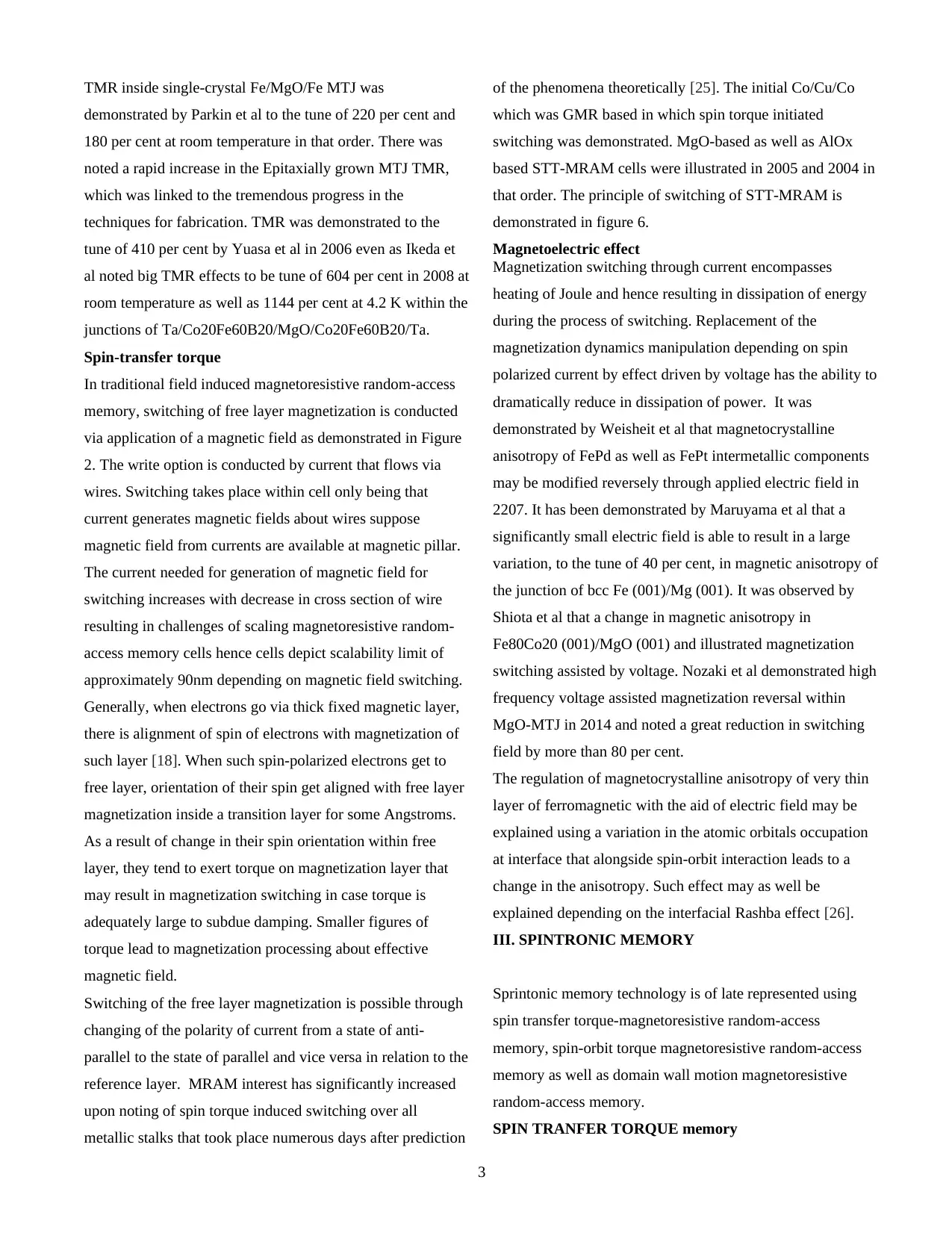
Spin-transfer torque
In traditional field induced magnetoresistive random-access
memory, switching of free layer magnetization is conducted
via application of a magnetic field as demonstrated in Figure
2. The write option is conducted by current that flows via
wires. Switching takes place within cell only being that
current generates magnetic fields about wires suppose
magnetic field from currents are available at magnetic pillar.
The current needed for generation of magnetic field for
switching increases with decrease in cross section of wire
resulting in challenges of scaling magnetoresistive random-
access memory cells hence cells depict scalability limit of
approximately 90nm depending on magnetic field switching.
Generally, when electrons go via thick fixed magnetic layer,
there is alignment of spin of electrons with magnetization of
such layer [18]. When such spin-polarized electrons get to
free layer, orientation of their spin get aligned with free layer
magnetization inside a transition layer for some Angstroms.
As a result of change in their spin orientation within free
layer, they tend to exert torque on magnetization layer that
may result in magnetization switching in case torque is
adequately large to subdue damping. Smaller figures of
torque lead to magnetization processing about effective
magnetic field.
Switching of the free layer magnetization is possible through
changing of the polarity of current from a state of anti-
parallel to the state of parallel and vice versa in relation to the
reference layer. MRAM interest has significantly increased
upon noting of spin torque induced switching over all
metallic stalks that took place numerous days after prediction
of the phenomena theoretically [25]. The initial Co/Cu/Co
which was GMR based in which spin torque initiated
switching was demonstrated. MgO-based as well as AlOx
based STT-MRAM cells were illustrated in 2005 and 2004 in
that order. The principle of switching of STT-MRAM is
demonstrated in figure 6.
Magnetoelectric effect
Magnetization switching through current encompasses
heating of Joule and hence resulting in dissipation of energy
during the process of switching. Replacement of the
magnetization dynamics manipulation depending on spin
polarized current by effect driven by voltage has the ability to
dramatically reduce in dissipation of power. It was
demonstrated by Weisheit et al that magnetocrystalline
anisotropy of FePd as well as FePt intermetallic components
may be modified reversely through applied electric field in
2207. It has been demonstrated by Maruyama et al that a
significantly small electric field is able to result in a large
variation, to the tune of 40 per cent, in magnetic anisotropy of
the junction of bcc Fe (001)/Mg (001). It was observed by
Shiota et al that a change in magnetic anisotropy in
Fe80Co20 (001)/MgO (001) and illustrated magnetization
switching assisted by voltage. Nozaki et al demonstrated high
frequency voltage assisted magnetization reversal within
MgO-MTJ in 2014 and noted a great reduction in switching
field by more than 80 per cent.
The regulation of magnetocrystalline anisotropy of very thin
layer of ferromagnetic with the aid of electric field may be
explained using a variation in the atomic orbitals occupation
at interface that alongside spin-orbit interaction leads to a
change in the anisotropy. Such effect may as well be
explained depending on the interfacial Rashba effect [26].
III. SPINTRONIC MEMORY
Sprintonic memory technology is of late represented using
spin transfer torque-magnetoresistive random-access
memory, spin-orbit torque magnetoresistive random-access
memory as well as domain wall motion magnetoresistive
random-access memory.
SPIN TRANFER TORQUE memory
3
demonstrated by Parkin et al to the tune of 220 per cent and
180 per cent at room temperature in that order. There was
noted a rapid increase in the Epitaxially grown MTJ TMR,
which was linked to the tremendous progress in the
techniques for fabrication. TMR was demonstrated to the
tune of 410 per cent by Yuasa et al in 2006 even as Ikeda et
al noted big TMR effects to be tune of 604 per cent in 2008 at
room temperature as well as 1144 per cent at 4.2 K within the
junctions of Ta/Co20Fe60B20/MgO/Co20Fe60B20/Ta.
Spin-transfer torque
In traditional field induced magnetoresistive random-access
memory, switching of free layer magnetization is conducted
via application of a magnetic field as demonstrated in Figure
2. The write option is conducted by current that flows via
wires. Switching takes place within cell only being that
current generates magnetic fields about wires suppose
magnetic field from currents are available at magnetic pillar.
The current needed for generation of magnetic field for
switching increases with decrease in cross section of wire
resulting in challenges of scaling magnetoresistive random-
access memory cells hence cells depict scalability limit of
approximately 90nm depending on magnetic field switching.
Generally, when electrons go via thick fixed magnetic layer,
there is alignment of spin of electrons with magnetization of
such layer [18]. When such spin-polarized electrons get to
free layer, orientation of their spin get aligned with free layer
magnetization inside a transition layer for some Angstroms.
As a result of change in their spin orientation within free
layer, they tend to exert torque on magnetization layer that
may result in magnetization switching in case torque is
adequately large to subdue damping. Smaller figures of
torque lead to magnetization processing about effective
magnetic field.
Switching of the free layer magnetization is possible through
changing of the polarity of current from a state of anti-
parallel to the state of parallel and vice versa in relation to the
reference layer. MRAM interest has significantly increased
upon noting of spin torque induced switching over all
metallic stalks that took place numerous days after prediction
of the phenomena theoretically [25]. The initial Co/Cu/Co
which was GMR based in which spin torque initiated
switching was demonstrated. MgO-based as well as AlOx
based STT-MRAM cells were illustrated in 2005 and 2004 in
that order. The principle of switching of STT-MRAM is
demonstrated in figure 6.
Magnetoelectric effect
Magnetization switching through current encompasses
heating of Joule and hence resulting in dissipation of energy
during the process of switching. Replacement of the
magnetization dynamics manipulation depending on spin
polarized current by effect driven by voltage has the ability to
dramatically reduce in dissipation of power. It was
demonstrated by Weisheit et al that magnetocrystalline
anisotropy of FePd as well as FePt intermetallic components
may be modified reversely through applied electric field in
2207. It has been demonstrated by Maruyama et al that a
significantly small electric field is able to result in a large
variation, to the tune of 40 per cent, in magnetic anisotropy of
the junction of bcc Fe (001)/Mg (001). It was observed by
Shiota et al that a change in magnetic anisotropy in
Fe80Co20 (001)/MgO (001) and illustrated magnetization
switching assisted by voltage. Nozaki et al demonstrated high
frequency voltage assisted magnetization reversal within
MgO-MTJ in 2014 and noted a great reduction in switching
field by more than 80 per cent.
The regulation of magnetocrystalline anisotropy of very thin
layer of ferromagnetic with the aid of electric field may be
explained using a variation in the atomic orbitals occupation
at interface that alongside spin-orbit interaction leads to a
change in the anisotropy. Such effect may as well be
explained depending on the interfacial Rashba effect [26].
III. SPINTRONIC MEMORY
Sprintonic memory technology is of late represented using
spin transfer torque-magnetoresistive random-access
memory, spin-orbit torque magnetoresistive random-access
memory as well as domain wall motion magnetoresistive
random-access memory.
SPIN TRANFER TORQUE memory
3
⊘ This is a preview!⊘
Do you want full access?
Subscribe today to unlock all pages.
Trusted by 1+ million students worldwide
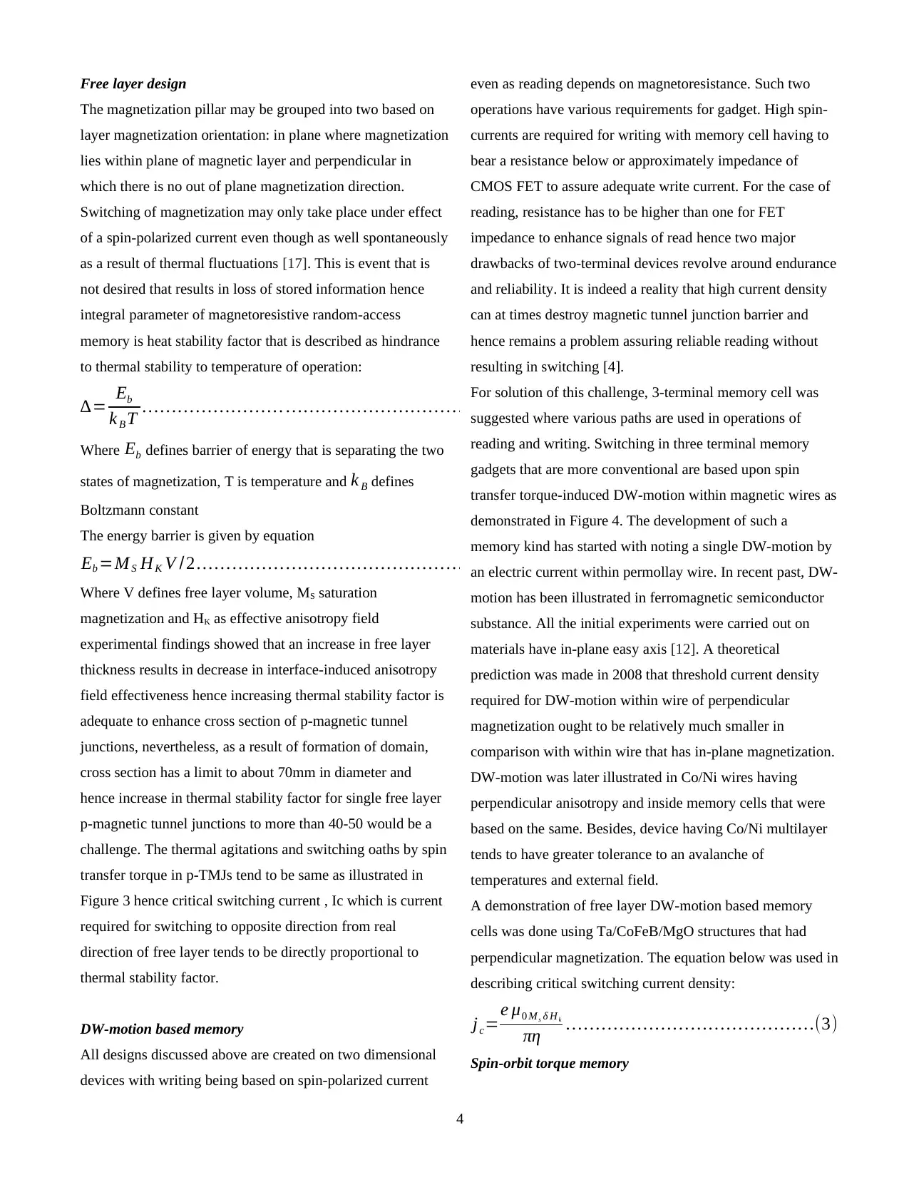
Free layer design
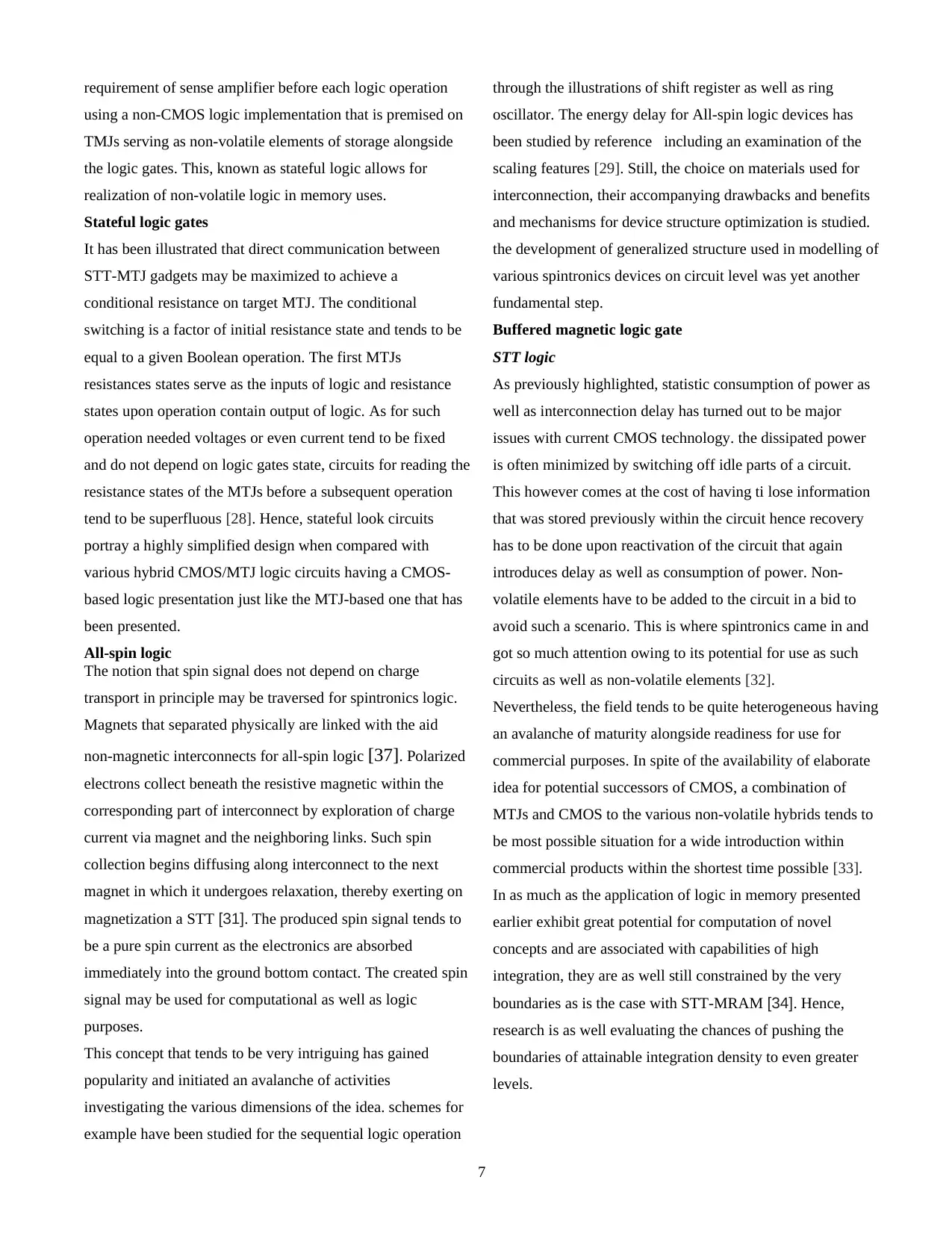
The magnetization pillar may be grouped into two based on
layer magnetization orientation: in plane where magnetization
lies within plane of magnetic layer and perpendicular in
which there is no out of plane magnetization direction.
Switching of magnetization may only take place under effect
of a spin-polarized current even though as well spontaneously
as a result of thermal fluctuations [17]. This is event that is
not desired that results in loss of stored information hence
integral parameter of magnetoresistive random-access
memory is heat stability factor that is described as hindrance
to thermal stability to temperature of operation:
∆= Eb
k B T … … … … … … … … …… … …… … …… … ….(1)
Where Eb defines barrier of energy that is separating the two
states of magnetization, T is temperature and k B defines
Boltzmann constant
The energy barrier is given by equation
Eb =M S HK V /2 … … … … … … … … … … … … … … … ..(2)
Where V defines free layer volume, MS saturation
magnetization and HK as effective anisotropy field
experimental findings showed that an increase in free layer
thickness results in decrease in interface-induced anisotropy
field effectiveness hence increasing thermal stability factor is
adequate to enhance cross section of p-magnetic tunnel
junctions, nevertheless, as a result of formation of domain,
cross section has a limit to about 70mm in diameter and
hence increase in thermal stability factor for single free layer
p-magnetic tunnel junctions to more than 40-50 would be a
challenge. The thermal agitations and switching oaths by spin
transfer torque in p-TMJs tend to be same as illustrated in
Figure 3 hence critical switching current , Ic which is current
required for switching to opposite direction from real
direction of free layer tends to be directly proportional to
thermal stability factor.
DW-motion based memory
All designs discussed above are created on two dimensional
devices with writing being based on spin-polarized current
even as reading depends on magnetoresistance. Such two
operations have various requirements for gadget. High spin-
currents are required for writing with memory cell having to
bear a resistance below or approximately impedance of
CMOS FET to assure adequate write current. For the case of
reading, resistance has to be higher than one for FET
impedance to enhance signals of read hence two major
drawbacks of two-terminal devices revolve around endurance
and reliability. It is indeed a reality that high current density
can at times destroy magnetic tunnel junction barrier and
hence remains a problem assuring reliable reading without
resulting in switching [4].
For solution of this challenge, 3-terminal memory cell was
suggested where various paths are used in operations of
reading and writing. Switching in three terminal memory
gadgets that are more conventional are based upon spin
transfer torque-induced DW-motion within magnetic wires as
demonstrated in Figure 4. The development of such a
memory kind has started with noting a single DW-motion by
an electric current within permollay wire. In recent past, DW-
motion has been illustrated in ferromagnetic semiconductor
substance. All the initial experiments were carried out on
materials have in-plane easy axis [12]. A theoretical
prediction was made in 2008 that threshold current density
required for DW-motion within wire of perpendicular
magnetization ought to be relatively much smaller in
comparison with within wire that has in-plane magnetization.
DW-motion was later illustrated in Co/Ni wires having
perpendicular anisotropy and inside memory cells that were
based on the same. Besides, device having Co/Ni multilayer
tends to have greater tolerance to an avalanche of
temperatures and external field.
A demonstration of free layer DW-motion based memory
cells was done using Ta/CoFeB/MgO structures that had
perpendicular magnetization. The equation below was used in
describing critical switching current density:
jc=e μ0 M s δ H k
πη … … … … … … … …… … … … … …(3)
Spin-orbit torque memory
4
Paraphrase This Document
Need a fresh take? Get an instant paraphrase of this document with our AI Paraphraser
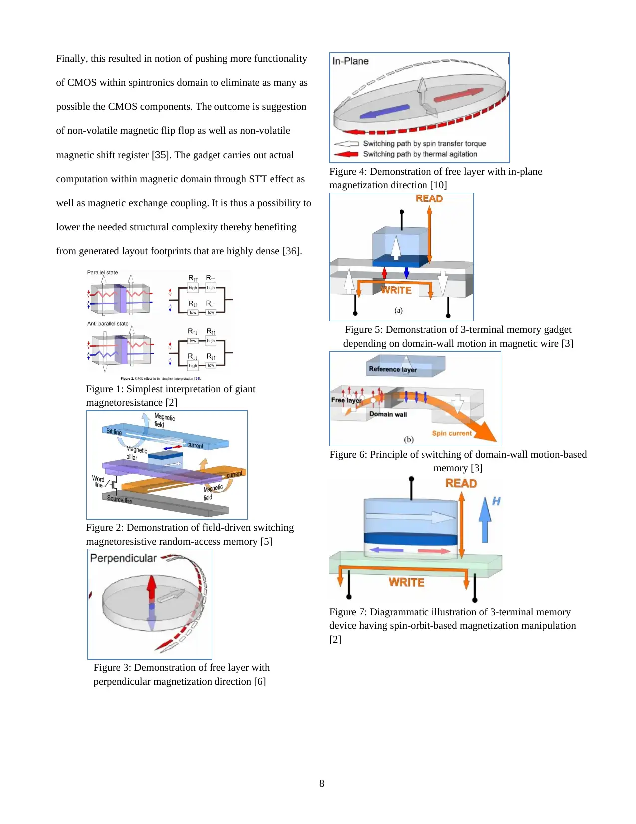
Manipulation of spin-orbit based magnetization is as well
ideal for creation of three terminal memory cells since
switching current doesn’t flow via barrier layer. A model
spin-orbit-based memory is magnetic tunnel junction
fabricated on heavy density metal pipe having large spin orbit
association in which free layer is directly linked with metal
pipe as demonstrated in Figure 5 & 6. The in-plane current
induces spin-torque via spin-orbit coupling effect with regard
to Rashba effect [15].
Another benefit of spin-orbit based memory revolves around
fact that it illustrates faster switching in comparison with spin
transfer torque switching. However, spin-orbit based memory
occupies more spaces since it needs a second transistor to
accomplish writing operations [5]. This second transistor
challenge may be sorted via preselection of single cells via
voltage pulse that is applied to cell at the same time with
powering spin Hall metal line. The voltage pulse serves to
make magnetic anisotropy soft of free layer of cell hence
hastening magnetization switching of preselected cell.
Nevertheless, this arrangement demands external magnetic
field.
IV. SPINTRONIC OSCILLATORS
Spin-based oscillators may be grouped into two as a factor of
physical phenomena used in exciting magnetization
processions within magnetic layer: Spin torque oscillators as
well as Hall nano-oscillators
Spin torque oscillators
A Spin torque oscillator is generally created by a GMR-pillar
or even magnetic tunnel junction. The magnetization
oscillation may be sensed in form of a high frequency voltage
by virtue of effect of TMR or GMR. The frequency of
procession of Spin torque oscillators is tunable within
relatively large range from 5 GHz to 45 GHz both via direct
current or even magnetic field that is applied hence spin
torque oscillators have relatively wide tenability in
comparison with voltage controlled oscillator and Yttrium
iron garnet oscillators. Another benefit of spin torque
oscillators is extreme small size [16].
It is estimated that a spin torque oscillators at least 50 times
smaller than ordinary LC-tank voltage controlled oscillator
which is designed in CMOS process, majorly as result of big
voltage controlled oscillator inductor footprint [6]. The spin
torque oscillator technology thus provides large frequency of
operation, low consumption of power as well as small size.
Still, spin torque oscillators have a significant potential for
numerous applications that are microwave-based for instance
fast modulators, broadband oscillators as well as sensitive
filed detectors.
Spin torque oscillators can further be differentiated by their
structure and grouped into nano-contact spin torque
oscillators where current goes via an extended magnetic
structure via a construction –NC and nano-pillar spin torque
oscillators [21]. Nano-contact spin torque oscillators have
been created in various geometries and may be grouped as
per number of NCs. The nano-pillar spin torque oscillators
can be categorized into perpendicular i.e. with-out-of plane
magnetization and in-plane i.e. with imagination along plane
of magnetic layer as influenced by orientation of free layer
magnetization.
Spin torque oscillators based on nano-pillars having in plane
magnetization demonstrate capabilities of high frequency
even though still require large external magnetic field and are
often associated with low levels of power output. Oscillators
having perpendicular magnetizations of free layer are found
to produce magnetization without need of external magnetic
field even though they are as well associated with
significantly low output power. Their functionality and
application are often limited by their low frequency of
operation which is 2GHz [7].
Proposal was made of bias-field-free spin torque oscillator
pegged on in-plane MgO-magnetic tunnel junction having
elliptical cross-section even though not ideal overlap between
layers of magnet and free layer. Nevertheless, shortcoming of
this architecture is on narrow frequency range as well as
weak dependence on current density. Still, alternative
structure pegged on two magnetic tunnel junctions having
shared free layer as demonstrated in Figure 7 that
demonstrates stable oscillations with relatively high
frequency without necessarily requiring external magnetics
field has been suggested. In structure, there is addition of
5
second magnetic tunnel junction in a bid to avoid switching
of free layer as well as encourage oscillatory conduct. The
frequency of operation of stable oscillations may be tuned in
broad range by changing density of currents that flow via
magnetic tunnel junction and it was demonstrated frequency
of oscillation of this structure might get to as high as 30GHz
[11].
As demonstrated by simulations, components based on two
magnetic tunnel junctions having a shared free layer as well
as with out-of-plane magnetization of free layer as well
illustrate stable oscillations. To this point, power produced by
spin torque oscillators is not adequate for applications with
conventional GMR based spin torque oscillator having output
power measured in sub-nW ranges.
Spin Hall nano-oscillator
Spin Hall nano-oscillator can be created by precession
produced by spin hall effect. A spin Hall nano-oscillator is
composed of a non-magnetic layer having high spin-orbit
coupling mounted at top of magnetic layer. The gadget might
produce microwave signal often within range of 2GHz to
10GHz important in telecommunication applications. The
gadgets adopt pure spin current made by spin hall effect
within non-magnetic layer and provide extremely low
consumption of power, smaller dimensions as well as broad
range of frequency compared with available technologies [8].
Spin Hall nano-oscillators have designed, illustrated and
fabricated in various geometries including nano-gap i.e. a
disk having triangular contacts, nano-construction as well as
nano wire as demonstrated in Figure 9.
Research has demonstrated that spin Hall nano-oscillators
depending on spin-current local injection showed
significantly large power as well as small-auto-oscillation
line width when subjected to cryogenic temperatures.
Nevertheless, both of such features reduce to great extent
when temperatures are increases as a result of excitation of
additional modes leading to thermal mode hopping at raised
temperatures [20].
Such effects are avoidable if just a single mode is excited
selectively for instance by modification of geometrical region
of auto-oscillation in controlled manner. Principally, one
would anticipate auto-oscillation region ought to be a factor
of experimental conditions for instance spins injection
geometry [9]. Nevertheless, in reality, such approach in
controlling auto-oscillation features may be challenging as
local injection of spin current in continuous magnetic film
results in spontaneous formation of bullet auto-oscillation
mode having spatial dimensions being determined by non-
linear self-localization effects as opposed to injection area of
spin current [22].
V. SPINTRONIC LOGIC
Spin-based gadgets are perceived one of the most promising
ways of going beyond the prevailing restrictions of state of
the art logic circuits based on CMOS. For example inclusion
of non-volatile components within logic circuits may be
applicable in the overcoming of the issue of standby power
dissipation that is fast growing. STT switched MTJs tend to
be very appropriate for logic applications of all the wide
variety of non-volatile technologies.
Logic-in memory
STT-MTJ-based logic circuits may in principle be
differentiated into two groups:
The initial group is the MTJ/CMOS circuits in which MTJs
serve as just buffer gadgets in storing computation outcomes.
Such MTJ/CMOS logic circuits generally adopt MTJs just for
the purposes of storage. CMOS segments still perform the
actual logic functions hence sense amplifiers are needed in
reading the data stored at every logic state as well as offering
the subsequent stage with enough current or even voltage
signal as the input. Such increases the count of the device as
well as has a dangerous impact on power consumption as
well as delay. There is as well no generalization plan for a
change to large scale logic systems alongside it is a great
challenge to make a direct comparison of the various hybrid
CMOS/MTJ logic circuits implementations. hence, an
elaborate as well as comprehensive study is needed in
benchmarking the various hybrid CMOS/MTJ logic circuits
against one another [27].
The second group goes beyond the aforementioned issues
through the use of MTJs in the capacity of the major
computing element. It is indeed a possibility to remove the
6
⊘ This is a preview!⊘
Do you want full access?
Subscribe today to unlock all pages.
Trusted by 1+ million students worldwide
requirement of sense amplifier before each logic operation
using a non-CMOS logic implementation that is premised on
TMJs serving as non-volatile elements of storage alongside
the logic gates. This, known as stateful logic allows for
realization of non-volatile logic in memory uses.
Stateful logic gates
It has been illustrated that direct communication between
STT-MTJ gadgets may be maximized to achieve a
conditional resistance on target MTJ. The conditional
switching is a factor of initial resistance state and tends to be
equal to a given Boolean operation. The first MTJs
resistances states serve as the inputs of logic and resistance
states upon operation contain output of logic. As for such
operation needed voltages or even current tend to be fixed
and do not depend on logic gates state, circuits for reading the
resistance states of the MTJs before a subsequent operation
tend to be superfluous [28]. Hence, stateful look circuits
portray a highly simplified design when compared with
various hybrid CMOS/MTJ logic circuits having a CMOS-
based logic presentation just like the MTJ-based one that has
been presented.
All-spin logic
The notion that spin signal does not depend on charge
transport in principle may be traversed for spintronics logic.
Magnets that separated physically are linked with the aid
non-magnetic interconnects for all-spin logic [37]. Polarized
electrons collect beneath the resistive magnetic within the
corresponding part of interconnect by exploration of charge
current via magnet and the neighboring links. Such spin
collection begins diffusing along interconnect to the next
magnet in which it undergoes relaxation, thereby exerting on
magnetization a STT [31]. The produced spin signal tends to
be a pure spin current as the electronics are absorbed
immediately into the ground bottom contact. The created spin
signal may be used for computational as well as logic
purposes.
This concept that tends to be very intriguing has gained
popularity and initiated an avalanche of activities
investigating the various dimensions of the idea. schemes for
example have been studied for the sequential logic operation
through the illustrations of shift register as well as ring
oscillator. The energy delay for All-spin logic devices has
been studied by reference including an examination of the
scaling features [29]. Still, the choice on materials used for
interconnection, their accompanying drawbacks and benefits
and mechanisms for device structure optimization is studied.
the development of generalized structure used in modelling of
various spintronics devices on circuit level was yet another
fundamental step.
Buffered magnetic logic gate
STT logic
As previously highlighted, statistic consumption of power as
well as interconnection delay has turned out to be major
issues with current CMOS technology. the dissipated power
is often minimized by switching off idle parts of a circuit.
This however comes at the cost of having ti lose information
that was stored previously within the circuit hence recovery
has to be done upon reactivation of the circuit that again
introduces delay as well as consumption of power. Non-
volatile elements have to be added to the circuit in a bid to
avoid such a scenario. This is where spintronics came in and
got so much attention owing to its potential for use as such
circuits as well as non-volatile elements [32].
Nevertheless, the field tends to be quite heterogeneous having
an avalanche of maturity alongside readiness for use for
commercial purposes. In spite of the availability of elaborate
idea for potential successors of CMOS, a combination of
MTJs and CMOS to the various non-volatile hybrids tends to
be most possible situation for a wide introduction within
commercial products within the shortest time possible [33].
In as much as the application of logic in memory presented
earlier exhibit great potential for computation of novel
concepts and are associated with capabilities of high
integration, they are as well still constrained by the very
boundaries as is the case with STT-MRAM [34]. Hence,
research is as well evaluating the chances of pushing the
boundaries of attainable integration density to even greater
levels.
7
Paraphrase This Document
Need a fresh take? Get an instant paraphrase of this document with our AI Paraphraser
Finally, this resulted in notion of pushing more functionality
of CMOS within spintronics domain to eliminate as many as
possible the CMOS components. The outcome is suggestion
of non-volatile magnetic flip flop as well as non-volatile
magnetic shift register [35]. The gadget carries out actual
computation within magnetic domain through STT effect as
well as magnetic exchange coupling. It is thus a possibility to
lower the needed structural complexity thereby benefiting
from generated layout footprints that are highly dense [36].
Figure 1: Simplest interpretation of giant
magnetoresistance [2]
Figure 2: Demonstration of field-driven switching
magnetoresistive random-access memory [5]
Figure 3: Demonstration of free layer with
perpendicular magnetization direction [6]
Figure 4: Demonstration of free layer with in-plane
magnetization direction [10]
Figure 5: Demonstration of 3-terminal memory gadget
depending on domain-wall motion in magnetic wire [3]
Figure 6: Principle of switching of domain-wall motion-based
memory [3]
Figure 7: Diagrammatic illustration of 3-terminal memory
device having spin-orbit-based magnetization manipulation
[2]
8
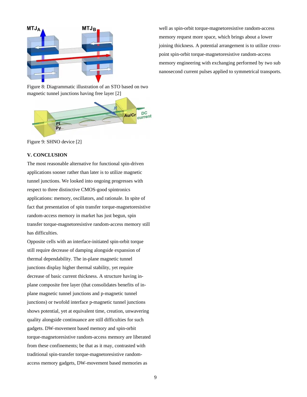
Figure 8: Diagrammatic illustration of an STO based on two
magnetic tunnel junctions having free layer [2]
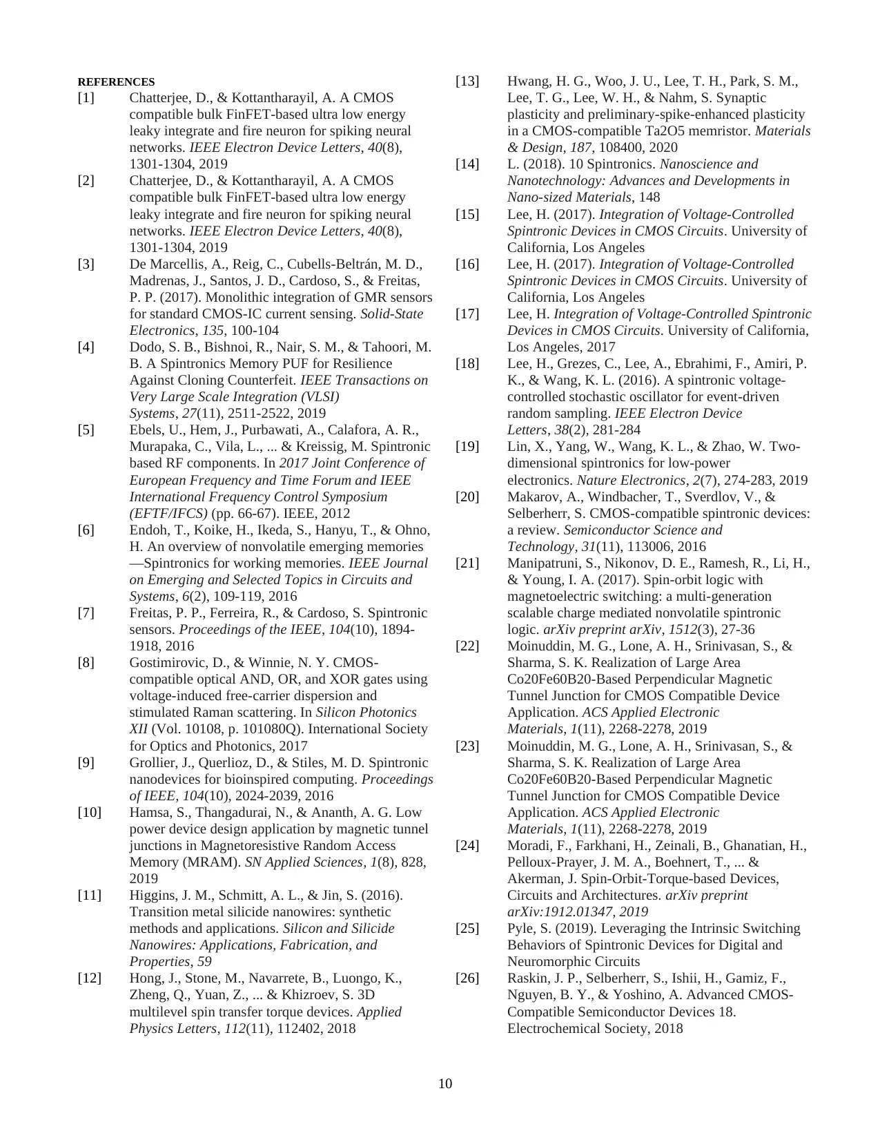
Figure 9: SHNO device [2]
V. CONCLUSION
The most reasonable alternative for functional spin-driven
applications sooner rather than later is to utilize magnetic
tunnel junctions. We looked into ongoing progresses with
respect to three distinctive CMOS-good spintronics
applications: memory, oscillators, and rationale. In spite of
fact that presentation of spin transfer torque-magnetoresistive
random-access memory in market has just begun, spin
transfer torque-magnetoresistive random-access memory still
has difficulties.
Opposite cells with an interface-initiated spin-orbit torque
still require decrease of damping alongside expansion of
thermal dependability. The in-plane magnetic tunnel
junctions display higher thermal stability, yet require
decrease of basic current thickness. A structure having in-
plane composite free layer (that consolidates benefits of in-
plane magnetic tunnel junctions and p-magnetic tunnel
junctions) or twofold interface p-magnetic tunnel junctions
shows potential, yet at equivalent time, creation, unwavering
quality alongside continuance are still difficulties for such
gadgets. DW-movement based memory and spin-orbit
torque-magnetoresistive random-access memory are liberated
from these confinements; be that as it may, contrasted with
traditional spin-transfer torque-magnetoresistive random-
access memory gadgets, DW-movement based memories as
well as spin-orbit torque-magnetoresistive random-access
memory request more space, which brings about a lower
joining thickness. A potential arrangement is to utilize cross-
point spin-orbit torque-magnetoresistive random-access
memory engineering with exchanging performed by two sub
nanosecond current pulses applied to symmetrical transports.
9
magnetic tunnel junctions having free layer [2]
Figure 9: SHNO device [2]
V. CONCLUSION
The most reasonable alternative for functional spin-driven
applications sooner rather than later is to utilize magnetic
tunnel junctions. We looked into ongoing progresses with
respect to three distinctive CMOS-good spintronics
applications: memory, oscillators, and rationale. In spite of
fact that presentation of spin transfer torque-magnetoresistive
random-access memory in market has just begun, spin
transfer torque-magnetoresistive random-access memory still
has difficulties.
Opposite cells with an interface-initiated spin-orbit torque
still require decrease of damping alongside expansion of
thermal dependability. The in-plane magnetic tunnel
junctions display higher thermal stability, yet require
decrease of basic current thickness. A structure having in-
plane composite free layer (that consolidates benefits of in-
plane magnetic tunnel junctions and p-magnetic tunnel
junctions) or twofold interface p-magnetic tunnel junctions
shows potential, yet at equivalent time, creation, unwavering
quality alongside continuance are still difficulties for such
gadgets. DW-movement based memory and spin-orbit
torque-magnetoresistive random-access memory are liberated
from these confinements; be that as it may, contrasted with
traditional spin-transfer torque-magnetoresistive random-
access memory gadgets, DW-movement based memories as
well as spin-orbit torque-magnetoresistive random-access
memory request more space, which brings about a lower
joining thickness. A potential arrangement is to utilize cross-
point spin-orbit torque-magnetoresistive random-access
memory engineering with exchanging performed by two sub
nanosecond current pulses applied to symmetrical transports.
9
⊘ This is a preview!⊘
Do you want full access?
Subscribe today to unlock all pages.
Trusted by 1+ million students worldwide
REFERENCES
[1] Chatterjee, D., & Kottantharayil, A. A CMOS
compatible bulk FinFET-based ultra low energy
leaky integrate and fire neuron for spiking neural
networks. IEEE Electron Device Letters, 40(8),
1301-1304, 2019
[2] Chatterjee, D., & Kottantharayil, A. A CMOS
compatible bulk FinFET-based ultra low energy
leaky integrate and fire neuron for spiking neural
networks. IEEE Electron Device Letters, 40(8),
1301-1304, 2019
[3] De Marcellis, A., Reig, C., Cubells-Beltrán, M. D.,
Madrenas, J., Santos, J. D., Cardoso, S., & Freitas,
P. P. (2017). Monolithic integration of GMR sensors
for standard CMOS-IC current sensing. Solid-State
Electronics, 135, 100-104
[4] Dodo, S. B., Bishnoi, R., Nair, S. M., & Tahoori, M.
B. A Spintronics Memory PUF for Resilience
Against Cloning Counterfeit. IEEE Transactions on
Very Large Scale Integration (VLSI)
Systems, 27(11), 2511-2522, 2019
[5] Ebels, U., Hem, J., Purbawati, A., Calafora, A. R.,
Murapaka, C., Vila, L., ... & Kreissig, M. Spintronic
based RF components. In 2017 Joint Conference of
European Frequency and Time Forum and IEEE
International Frequency Control Symposium
(EFTF/IFCS) (pp. 66-67). IEEE, 2012
[6] Endoh, T., Koike, H., Ikeda, S., Hanyu, T., & Ohno,
H. An overview of nonvolatile emerging memories
—Spintronics for working memories. IEEE Journal
on Emerging and Selected Topics in Circuits and
Systems, 6(2), 109-119, 2016
[7] Freitas, P. P., Ferreira, R., & Cardoso, S. Spintronic
sensors. Proceedings of the IEEE, 104(10), 1894-
1918, 2016
[8] Gostimirovic, D., & Winnie, N. Y. CMOS-
compatible optical AND, OR, and XOR gates using
voltage-induced free-carrier dispersion and
stimulated Raman scattering. In Silicon Photonics
XII (Vol. 10108, p. 101080Q). International Society
for Optics and Photonics, 2017
[9] Grollier, J., Querlioz, D., & Stiles, M. D. Spintronic
nanodevices for bioinspired computing. Proceedings
of IEEE, 104(10), 2024-2039, 2016
[10] Hamsa, S., Thangadurai, N., & Ananth, A. G. Low
power device design application by magnetic tunnel
junctions in Magnetoresistive Random Access
Memory (MRAM). SN Applied Sciences, 1(8), 828,
2019
[11] Higgins, J. M., Schmitt, A. L., & Jin, S. (2016).
Transition metal silicide nanowires: synthetic
methods and applications. Silicon and Silicide
Nanowires: Applications, Fabrication, and
Properties, 59
[12] Hong, J., Stone, M., Navarrete, B., Luongo, K.,
Zheng, Q., Yuan, Z., ... & Khizroev, S. 3D
multilevel spin transfer torque devices. Applied
Physics Letters, 112(11), 112402, 2018
[13] Hwang, H. G., Woo, J. U., Lee, T. H., Park, S. M.,
Lee, T. G., Lee, W. H., & Nahm, S. Synaptic
plasticity and preliminary-spike-enhanced plasticity
in a CMOS-compatible Ta2O5 memristor. Materials
& Design, 187, 108400, 2020
[14] L. (2018). 10 Spintronics. Nanoscience and
Nanotechnology: Advances and Developments in
Nano-sized Materials, 148
[15] Lee, H. (2017). Integration of Voltage-Controlled
Spintronic Devices in CMOS Circuits. University of
California, Los Angeles
[16] Lee, H. (2017). Integration of Voltage-Controlled
Spintronic Devices in CMOS Circuits. University of
California, Los Angeles
[17] Lee, H. Integration of Voltage-Controlled Spintronic
Devices in CMOS Circuits. University of California,
Los Angeles, 2017
[18] Lee, H., Grezes, C., Lee, A., Ebrahimi, F., Amiri, P.
K., & Wang, K. L. (2016). A spintronic voltage-
controlled stochastic oscillator for event-driven
random sampling. IEEE Electron Device
Letters, 38(2), 281-284
[19] Lin, X., Yang, W., Wang, K. L., & Zhao, W. Two-
dimensional spintronics for low-power
electronics. Nature Electronics, 2(7), 274-283, 2019
[20] Makarov, A., Windbacher, T., Sverdlov, V., &
Selberherr, S. CMOS-compatible spintronic devices:
a review. Semiconductor Science and
Technology, 31(11), 113006, 2016
[21] Manipatruni, S., Nikonov, D. E., Ramesh, R., Li, H.,
& Young, I. A. (2017). Spin-orbit logic with
magnetoelectric switching: a multi-generation
scalable charge mediated nonvolatile spintronic
logic. arXiv preprint arXiv, 1512(3), 27-36
[22] Moinuddin, M. G., Lone, A. H., Srinivasan, S., &
Sharma, S. K. Realization of Large Area
Co20Fe60B20-Based Perpendicular Magnetic
Tunnel Junction for CMOS Compatible Device
Application. ACS Applied Electronic
Materials, 1(11), 2268-2278, 2019
[23] Moinuddin, M. G., Lone, A. H., Srinivasan, S., &
Sharma, S. K. Realization of Large Area
Co20Fe60B20-Based Perpendicular Magnetic
Tunnel Junction for CMOS Compatible Device
Application. ACS Applied Electronic
Materials, 1(11), 2268-2278, 2019
[24] Moradi, F., Farkhani, H., Zeinali, B., Ghanatian, H.,
Pelloux-Prayer, J. M. A., Boehnert, T., ... &
Akerman, J. Spin-Orbit-Torque-based Devices,
Circuits and Architectures. arXiv preprint
arXiv:1912.01347, 2019
[25] Pyle, S. (2019). Leveraging the Intrinsic Switching
Behaviors of Spintronic Devices for Digital and
Neuromorphic Circuits
[26] Raskin, J. P., Selberherr, S., Ishii, H., Gamiz, F.,
Nguyen, B. Y., & Yoshino, A. Advanced CMOS-
Compatible Semiconductor Devices 18.
Electrochemical Society, 2018
10
Paraphrase This Document
Need a fresh take? Get an instant paraphrase of this document with our AI Paraphraser
[27] Shahsavari, M., & Boulet, P. (2017). Memristor
nanodevice for unconventional computing: review
and applications. arXiv preprint arXiv:1703.00331
[28] Singh, P., & Kumar, S. (2019). Laser-assisted stress
reduction in molybdenum microstructures for
CMOS compatible MEMS integration. Sensors and
Actuators A: Physical, 295, 523-531
[29] Sverdlov, V., & Selberherr, S. CMOS Technology
Compatible Magnetic Memories. In 2019 8th
International Symposium on Next Generation
Electronics (ISNE) (pp. 1-2). IEEE, 2019
[30] Sverdlov, V., & Selberherr, S. Demands for spin-
based nonvolatility in emerging digital logic and
memory devices for low power computing. Facta
Universitatis, Series: Electronics and
Energetics, 31(4), 529-545, 2018
[31] Sverdlov, V., & Selberherr, S. Spin-Based CMOS-
Compatible Memories. In 2019 IEEE 9th
International Nanoelectronics Conferences
(INEC) (pp. 1-2). IEEE, 2019
[32] , V., Osintsev, D., & Selberherr, S. (2016). Silicon-
on-insulator for spintronic applications: spin lifetime
and electric spin manipulation. Physical Sciences
Reviews, 1(5)
[33] Torunbalci, M. M., Upadhyaya, P., Bhave, S. A., &
Camsari, K. Y. Modular Compact Modeling of
Magnetic Tunnel Junction Devices. arXiv preprint
arXiv:1805.00066, 2018
[34] Wang, Y. (2017). Reliability analysis of spintronic
device based logic and memory circuits (Doctoral
dissertation)
[35] Xiong, K. Design, Fabrication, Characterization and
Modeling of CMOS-Compatible PtSe2 MOSFETs,
2020
[36] Zahedinejad, M., Mazraati, H., Fulara, H., Yue, J.,
Jiang, S., Awad, A. A., & Åkerman, J. (2018).
CMOS compatible W/CoFeB/MgO spin Hall nano-
oscillators with wide frequency tunability. Applied
Physics Letters, 112(13), 132404
[37] Zhang, Y., Fan, J., Huang, Q., Zhu, J., Zhao, Y., Li,
M., ... & Huang, R. (2018). Voltage-Controlled
Magnetoresistance in Silicon Nanowire
Transistors. Scientific reports, 8(1), 1-7
11
1 out of 11
Your All-in-One AI-Powered Toolkit for Academic Success.
+13062052269
info@desklib.com
Available 24*7 on WhatsApp / Email
![[object Object]](/_next/static/media/star-bottom.7253800d.svg)
Unlock your academic potential
Copyright © 2020–2026 A2Z Services. All Rights Reserved. Developed and managed by ZUCOL.