Electrical Engineering Report: Semiconductor Devices and Applications
VerifiedAdded on 2022/11/29
|12
|2546
|244
Report
AI Summary
This report provides a comprehensive overview of semiconductor devices, focusing on the operation and applications of bipolar junction transistors (BJTs) and junction field-effect transistors (JFETs). The report begins with an introduction to semiconductor materials and the basic principles of diodes, including their current-voltage characteristics. It then delves into the construction and operation of BJTs, explaining the different regions of operation (cutoff, saturation, and active) and deriving relevant equations for current and voltage gain. The report further explores JFETs, discussing their types, operating regions (ohmic, cutoff, saturation, and breakdown), and voltage-current characteristics. The methodology section describes the use of Proteus software to simulate and analyze BJT and JFET circuits, with detailed results and discussions on the observed behavior of these devices, including current and voltage gain calculations. Finally, the report touches upon the application of semiconductor devices in voltage regulators, specifically the emitter follower regulator.
Running head: SEMICONDUCTOR DEVICES AND ITS APPLICATIONS 1
SEMICONDUCTOR DEVICES AND ITS APPLICATIONS
SEMICONDUCTOR DEVICES AND ITS APPLICATIONS
Paraphrase This Document
Need a fresh take? Get an instant paraphrase of this document with our AI Paraphraser
SEMICONDUCTOR DEVICES AND ITS APPLICATIONS
2
OBJECTIVES
To investigate how bipolar junction transistor operates
To investigate how junction field effect transistor operates
To carry out investigation on operation of series voltage regulator
THEORY
Semiconductor device is a component used in electronics, it is made from semi-conductor
material such as silicon, gallium arsenide and germanium. These devices are used in my
applications since they are cheap, reliable and compact (Britannica, n.d). Semiconductor devices
are used in power devices, optical sensors among other applications and are key components in
communication, control and data-processing systems. These devices are popular due to their
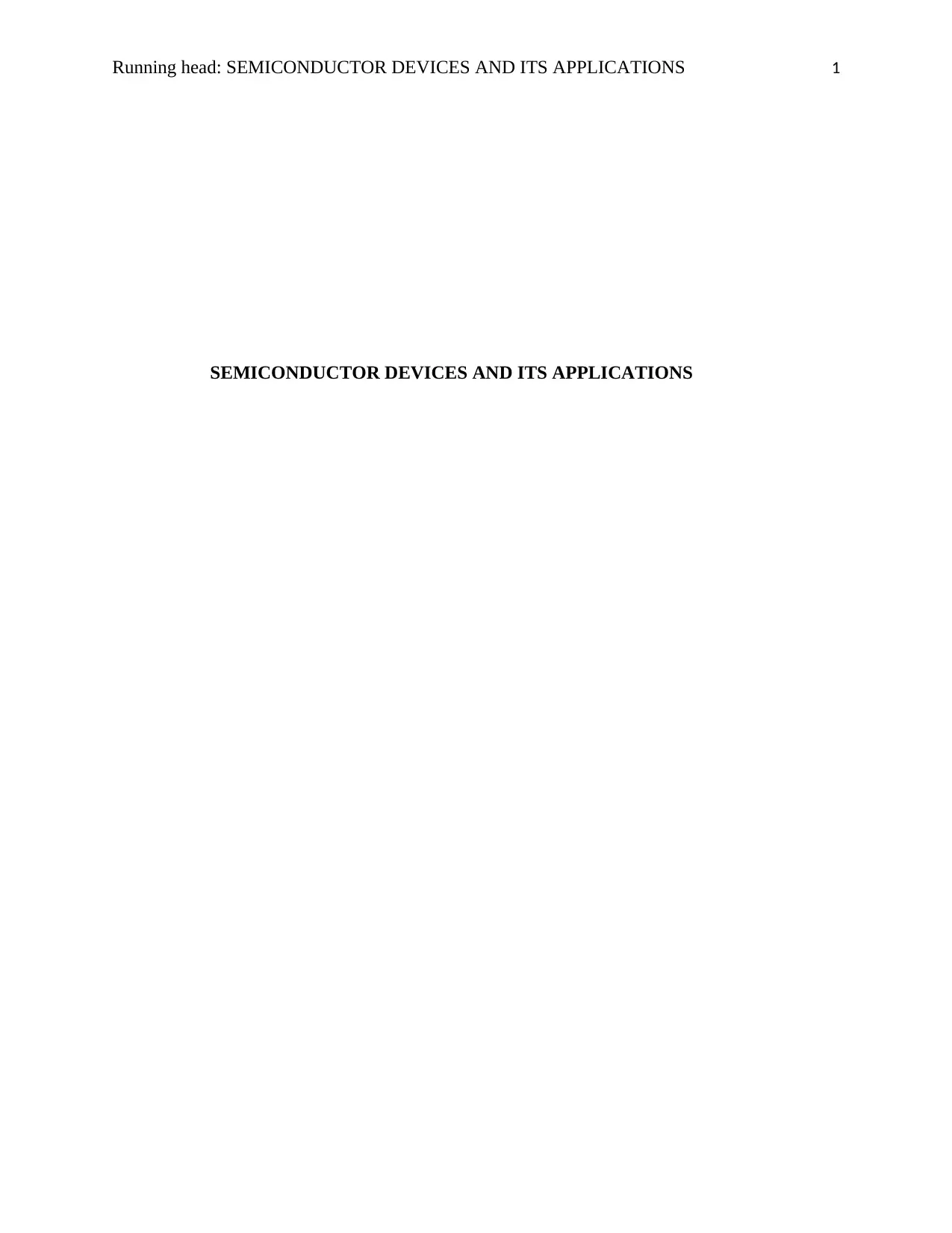
wide range of current and voltage ratings (Elprocus, n.d), figure 1 below show examples of
semiconductor devices and are made up of operational amplifiers, resistors, diodes, transistors
and ICs.
Figure 1: semiconductor devices obtained from ELPROCUS electronics (online),
https://www.elprocus.com/semiconductor-devices-types-and-applications/ on 7th of September
2019.
Semi-conductor device properties can be easily change to suit specified application, by adding
impurities to it, this process help to increase the number of holes or electrons within the
semiconductor. Conductivity of semiconductor devices are controlled by exposing it to heat or
light, by deforming doped grid or by electromagnetic field, thus they can be utilized in making
sensors (Elprocus, n.d). Semiconductor devices conducts current courtesy of holes and electrons,
popularly known as charge carriers.
Doping the semiconductor changes its properties, it either makes the holes or electrons to be in
excess. Semiconductor is known as p-type if it has excess holes and n-type if it contains excess
electrons. P-type and n-type semiconductor can be put together to form a junction, for example a
junction called p-n is formed when p and n-type semiconductors are joined.
2
OBJECTIVES
To investigate how bipolar junction transistor operates
To investigate how junction field effect transistor operates
To carry out investigation on operation of series voltage regulator
THEORY
Semiconductor device is a component used in electronics, it is made from semi-conductor
material such as silicon, gallium arsenide and germanium. These devices are used in my
applications since they are cheap, reliable and compact (Britannica, n.d). Semiconductor devices
are used in power devices, optical sensors among other applications and are key components in
communication, control and data-processing systems. These devices are popular due to their
wide range of current and voltage ratings (Elprocus, n.d), figure 1 below show examples of
semiconductor devices and are made up of operational amplifiers, resistors, diodes, transistors
and ICs.
Figure 1: semiconductor devices obtained from ELPROCUS electronics (online),
https://www.elprocus.com/semiconductor-devices-types-and-applications/ on 7th of September
2019.
Semi-conductor device properties can be easily change to suit specified application, by adding
impurities to it, this process help to increase the number of holes or electrons within the
semiconductor. Conductivity of semiconductor devices are controlled by exposing it to heat or
light, by deforming doped grid or by electromagnetic field, thus they can be utilized in making
sensors (Elprocus, n.d). Semiconductor devices conducts current courtesy of holes and electrons,
popularly known as charge carriers.
Doping the semiconductor changes its properties, it either makes the holes or electrons to be in
excess. Semiconductor is known as p-type if it has excess holes and n-type if it contains excess
electrons. P-type and n-type semiconductor can be put together to form a junction, for example a
junction called p-n is formed when p and n-type semiconductors are joined.
SEMICONDUCTOR DEVICES AND ITS APPLICATIONS
3
Diodes.
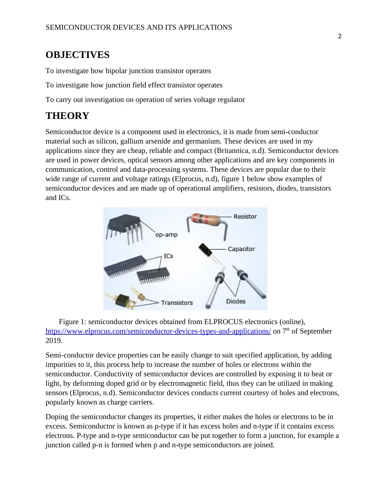
Figure 2 below shows current-voltage characteristics of a p-n junction
Figure 2: current-voltage characteristics of a silicon p-n junction. Obtained from britannica
electronics, https://www.britannica.com/technology/semiconductor-device/The-p-n-junction,
retrieved on 7th of September 2019
Section B represent a region of forward bias, in forward biasing positive of the supply is
connected to the positive of the junction and negative of the supply to the negative side of the
supply. For a flow of current to be successful, majority of the charge carriers must cross the
junction. For reverse bias in section c, p-side of the semi-conductor is connected to negative
voltage, and the charge carriers will move away from the junction hindering the flow of electrons
as depletion region is increased. When a semi-conductor is exposed to light, it increases the
production of charge carriers and in turn increases the conductivity. Diodes are being used to
generate light and as light-emitting diodes. The symbol of a diode is as shown in section D of
figure 2.
BIPOLAR TRANSISTORS
The bipolar transistor is a semi-conductor component that utilizes both electrons and holes in the
process of conduction (ElectronicsTutorial, n.d). This device is formed by two positive-negative
junctions, either a p-n-p or n-p-n arrangement. The middle region forms the base and the other
regions form the collector and emitter. Output current produced by the bipolar transistor depends
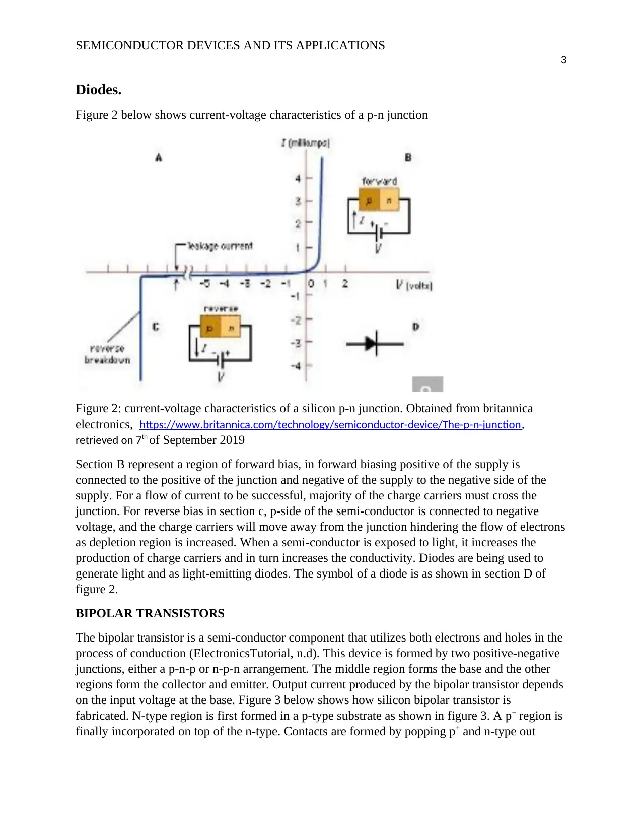
on the input voltage at the base. Figure 3 below shows how silicon bipolar transistor is
fabricated. N-type region is first formed in a p-type substrate as shown in figure 3. A p+ region is
finally incorporated on top of the n-type. Contacts are formed by popping p+ and n-type out
3
Diodes.
Figure 2 below shows current-voltage characteristics of a p-n junction
Figure 2: current-voltage characteristics of a silicon p-n junction. Obtained from britannica
electronics, https://www.britannica.com/technology/semiconductor-device/The-p-n-junction,
retrieved on 7th of September 2019
Section B represent a region of forward bias, in forward biasing positive of the supply is
connected to the positive of the junction and negative of the supply to the negative side of the
supply. For a flow of current to be successful, majority of the charge carriers must cross the
junction. For reverse bias in section c, p-side of the semi-conductor is connected to negative
voltage, and the charge carriers will move away from the junction hindering the flow of electrons
as depletion region is increased. When a semi-conductor is exposed to light, it increases the
production of charge carriers and in turn increases the conductivity. Diodes are being used to
generate light and as light-emitting diodes. The symbol of a diode is as shown in section D of
figure 2.
BIPOLAR TRANSISTORS
The bipolar transistor is a semi-conductor component that utilizes both electrons and holes in the
process of conduction (ElectronicsTutorial, n.d). This device is formed by two positive-negative
junctions, either a p-n-p or n-p-n arrangement. The middle region forms the base and the other
regions form the collector and emitter. Output current produced by the bipolar transistor depends
on the input voltage at the base. Figure 3 below shows how silicon bipolar transistor is
fabricated. N-type region is first formed in a p-type substrate as shown in figure 3. A p+ region is
finally incorporated on top of the n-type. Contacts are formed by popping p+ and n-type out
⊘ This is a preview!⊘
Do you want full access?
Subscribe today to unlock all pages.
Trusted by 1+ million students worldwide
SEMICONDUCTOR DEVICES AND ITS APPLICATIONS
4
through the insulator at the top as the emitter and base respectively. Another contact is made to
the p-region at the bottom (collector) as shown in figure 3 (A).
Figure 3 : A & B bipolar transistor, C symbols for p-n-p and n-p-n obtained from britannica
electronics, https://www.britannica.com/technology/semiconductor-device/The-p-n-junction,
retrieved on 7th of September 2019
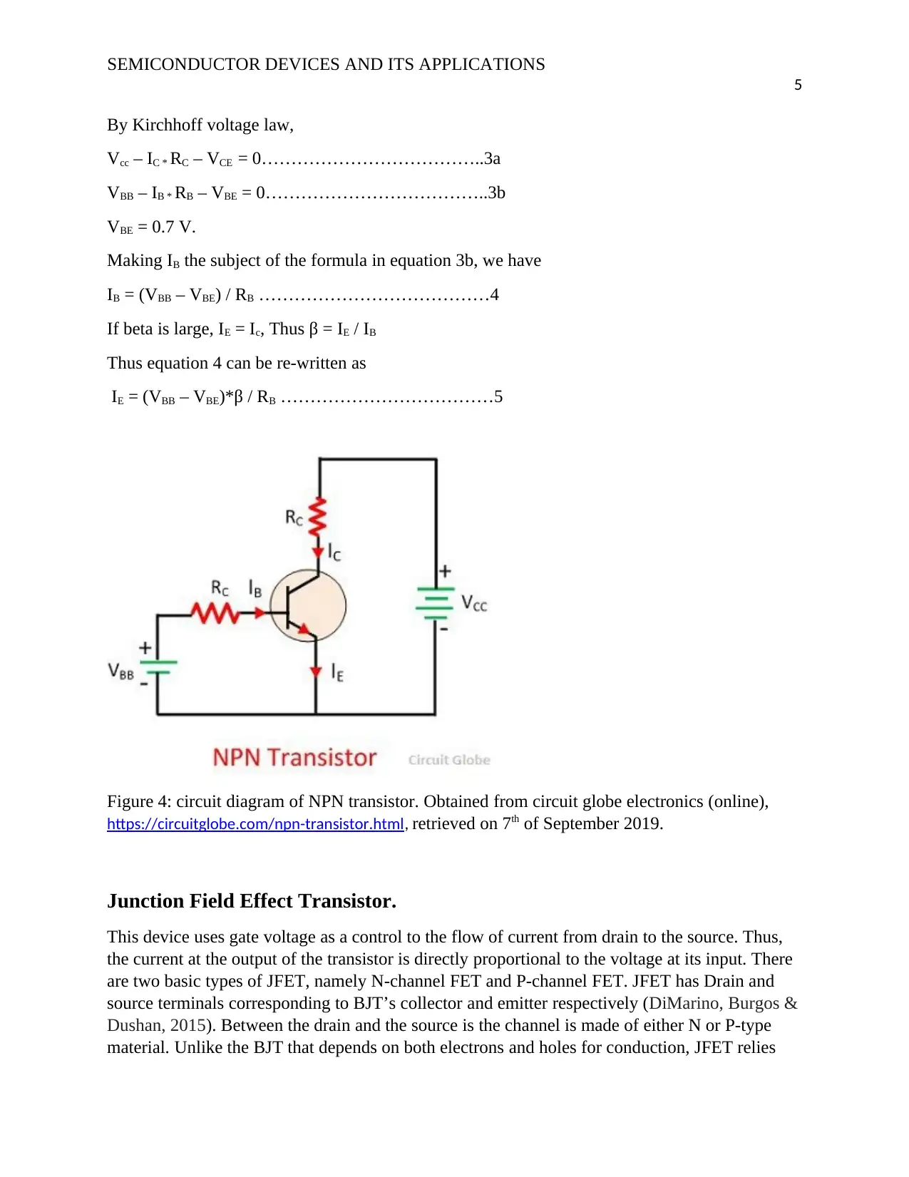
NPN Transistor
The circuit diagram of figure 4 utilizes an NPN transistor. Base and emitter circuit are forward-
biased whereas the base and collector circuit are reversed-biased. Normally, the collector is
connected to the positive terminal of voltage supply and the base to the negative of power supply
as to control on and off states of the transistor. The collector of the transistor is connected to the
power supply via a resistor Rc to regulate the amount of current flowing into the transistor.
Another resistor is connected to the base to limit the flow of current to the base (circuit globe,
n.d).
Bipolar transistor operates in three regions namely: cutoff, saturation and active region
(Nawaz, Chen, Chimento & Wang, 2016). In cutoff region, the transistor is inactive and no
current will be able to flow through it thus there is no current flowing through the base and
collector and the base voltage (Vbe) is less than 0.7. In saturation region, the transistor appears
like a short circuit between the emitter and collector. In this region base emitter voltage is equal
or greater that 0.7 V. in active region, the transistor act as linear amplifier. Voltage across the
emitter and collector is between 0.2 and the value of voltage source.
The following equations are deduced from the circuit of figure 4 when the transistor is in active
region
DC current gain, β = Ic/Ib………………………………………….…..1
By Kirchhoff current law, IB +………………………..2
4
through the insulator at the top as the emitter and base respectively. Another contact is made to
the p-region at the bottom (collector) as shown in figure 3 (A).
Figure 3 : A & B bipolar transistor, C symbols for p-n-p and n-p-n obtained from britannica
electronics, https://www.britannica.com/technology/semiconductor-device/The-p-n-junction,
retrieved on 7th of September 2019
NPN Transistor
The circuit diagram of figure 4 utilizes an NPN transistor. Base and emitter circuit are forward-
biased whereas the base and collector circuit are reversed-biased. Normally, the collector is
connected to the positive terminal of voltage supply and the base to the negative of power supply
as to control on and off states of the transistor. The collector of the transistor is connected to the
power supply via a resistor Rc to regulate the amount of current flowing into the transistor.
Another resistor is connected to the base to limit the flow of current to the base (circuit globe,
n.d).
Bipolar transistor operates in three regions namely: cutoff, saturation and active region
(Nawaz, Chen, Chimento & Wang, 2016). In cutoff region, the transistor is inactive and no
current will be able to flow through it thus there is no current flowing through the base and
collector and the base voltage (Vbe) is less than 0.7. In saturation region, the transistor appears
like a short circuit between the emitter and collector. In this region base emitter voltage is equal
or greater that 0.7 V. in active region, the transistor act as linear amplifier. Voltage across the
emitter and collector is between 0.2 and the value of voltage source.
The following equations are deduced from the circuit of figure 4 when the transistor is in active
region
DC current gain, β = Ic/Ib………………………………………….…..1
By Kirchhoff current law, IB +………………………..2
Paraphrase This Document
Need a fresh take? Get an instant paraphrase of this document with our AI Paraphraser
SEMICONDUCTOR DEVICES AND ITS APPLICATIONS
5
By Kirchhoff voltage law,
Vcc – IC * RC – VCE = 0………………………………..3a
VBB – IB * RB – VBE = 0………………………………..3b
VBE = 0.7 V.
Making IB the subject of the formula in equation 3b, we have
IB = (VBB – VBE) / RB …………………………………4
If beta is large, IE = Ic, Thus β = IE / IB
Thus equation 4 can be re-written as
IE = (VBB – VBE)*β / RB ………………………………5
Figure 4: circuit diagram of NPN transistor. Obtained from circuit globe electronics (online),
https://circuitglobe.com/npn-transistor.html, retrieved on 7th of September 2019.
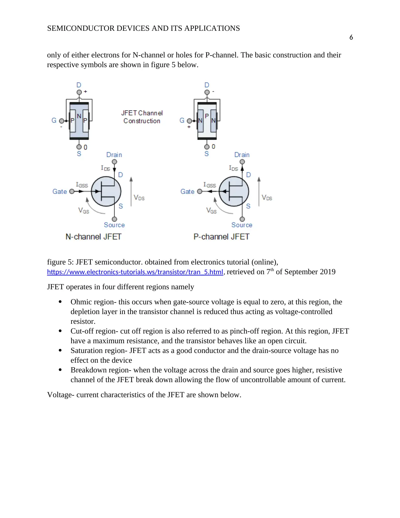
Junction Field Effect Transistor.
This device uses gate voltage as a control to the flow of current from drain to the source. Thus,
the current at the output of the transistor is directly proportional to the voltage at its input. There
are two basic types of JFET, namely N-channel FET and P-channel FET. JFET has Drain and
source terminals corresponding to BJT’s collector and emitter respectively (DiMarino, Burgos &
Dushan, 2015). Between the drain and the source is the channel is made of either N or P-type
material. Unlike the BJT that depends on both electrons and holes for conduction, JFET relies
5
By Kirchhoff voltage law,
Vcc – IC * RC – VCE = 0………………………………..3a
VBB – IB * RB – VBE = 0………………………………..3b
VBE = 0.7 V.
Making IB the subject of the formula in equation 3b, we have
IB = (VBB – VBE) / RB …………………………………4
If beta is large, IE = Ic, Thus β = IE / IB
Thus equation 4 can be re-written as
IE = (VBB – VBE)*β / RB ………………………………5
Figure 4: circuit diagram of NPN transistor. Obtained from circuit globe electronics (online),
https://circuitglobe.com/npn-transistor.html, retrieved on 7th of September 2019.
Junction Field Effect Transistor.
This device uses gate voltage as a control to the flow of current from drain to the source. Thus,
the current at the output of the transistor is directly proportional to the voltage at its input. There
are two basic types of JFET, namely N-channel FET and P-channel FET. JFET has Drain and
source terminals corresponding to BJT’s collector and emitter respectively (DiMarino, Burgos &
Dushan, 2015). Between the drain and the source is the channel is made of either N or P-type
material. Unlike the BJT that depends on both electrons and holes for conduction, JFET relies
SEMICONDUCTOR DEVICES AND ITS APPLICATIONS
6
only of either electrons for N-channel or holes for P-channel. The basic construction and their
respective symbols are shown in figure 5 below.
figure 5: JFET semiconductor. obtained from electronics tutorial (online),
https://www.electronics-tutorials.ws/transistor/tran_5.html, retrieved on 7th of September 2019
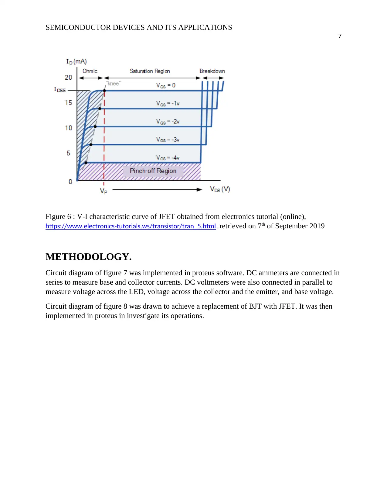
JFET operates in four different regions namely
Ohmic region- this occurs when gate-source voltage is equal to zero, at this region, the
depletion layer in the transistor channel is reduced thus acting as voltage-controlled
resistor.
Cut-off region- cut off region is also referred to as pinch-off region. At this region, JFET
have a maximum resistance, and the transistor behaves like an open circuit.
Saturation region- JFET acts as a good conductor and the drain-source voltage has no
effect on the device
Breakdown region- when the voltage across the drain and source goes higher, resistive
channel of the JFET break down allowing the flow of uncontrollable amount of current.
Voltage- current characteristics of the JFET are shown below.
6
only of either electrons for N-channel or holes for P-channel. The basic construction and their
respective symbols are shown in figure 5 below.
figure 5: JFET semiconductor. obtained from electronics tutorial (online),
https://www.electronics-tutorials.ws/transistor/tran_5.html, retrieved on 7th of September 2019
JFET operates in four different regions namely
Ohmic region- this occurs when gate-source voltage is equal to zero, at this region, the
depletion layer in the transistor channel is reduced thus acting as voltage-controlled
resistor.
Cut-off region- cut off region is also referred to as pinch-off region. At this region, JFET
have a maximum resistance, and the transistor behaves like an open circuit.
Saturation region- JFET acts as a good conductor and the drain-source voltage has no
effect on the device
Breakdown region- when the voltage across the drain and source goes higher, resistive
channel of the JFET break down allowing the flow of uncontrollable amount of current.
Voltage- current characteristics of the JFET are shown below.
⊘ This is a preview!⊘
Do you want full access?
Subscribe today to unlock all pages.
Trusted by 1+ million students worldwide
SEMICONDUCTOR DEVICES AND ITS APPLICATIONS
7
Figure 6 : V-I characteristic curve of JFET obtained from electronics tutorial (online),
https://www.electronics-tutorials.ws/transistor/tran_5.html, retrieved on 7th of September 2019
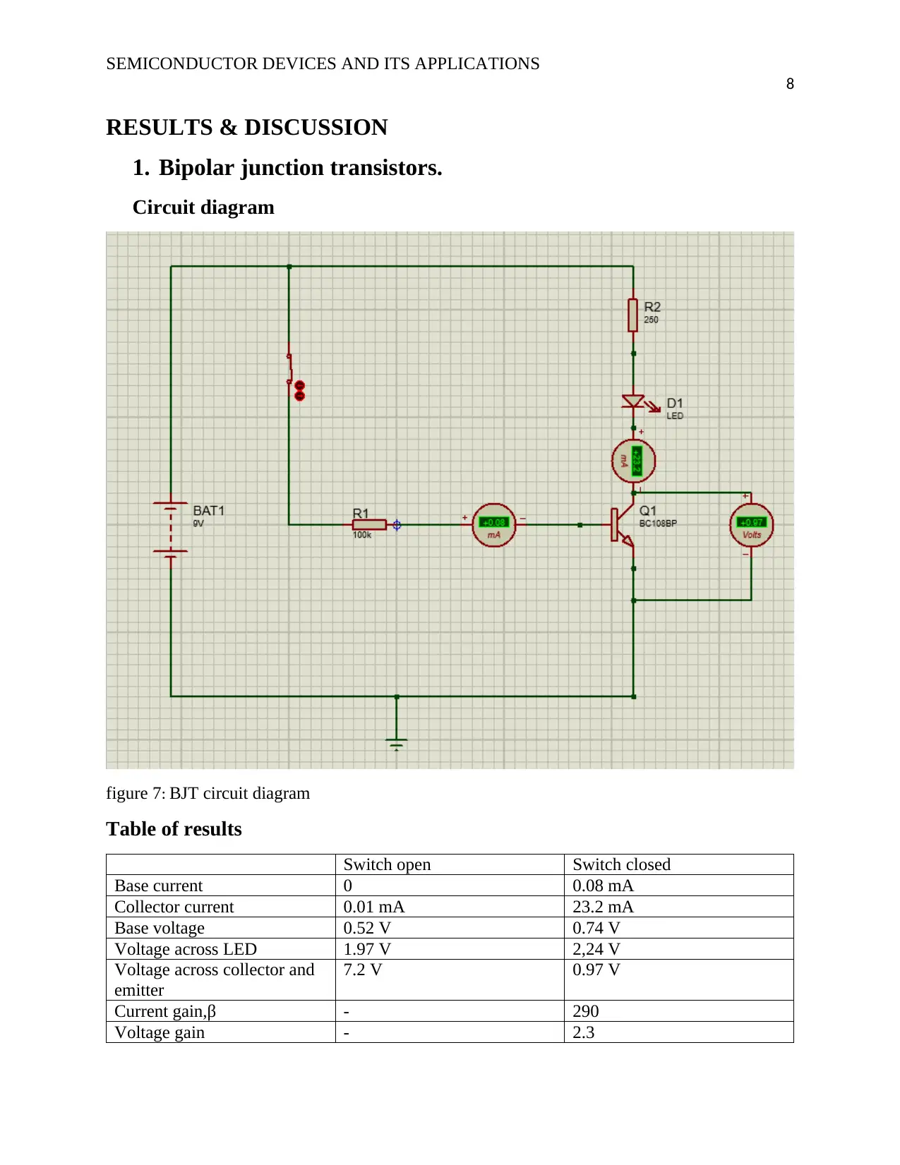
METHODOLOGY.
Circuit diagram of figure 7 was implemented in proteus software. DC ammeters are connected in
series to measure base and collector currents. DC voltmeters were also connected in parallel to
measure voltage across the LED, voltage across the collector and the emitter, and base voltage.
Circuit diagram of figure 8 was drawn to achieve a replacement of BJT with JFET. It was then
implemented in proteus in investigate its operations.
7
Figure 6 : V-I characteristic curve of JFET obtained from electronics tutorial (online),
https://www.electronics-tutorials.ws/transistor/tran_5.html, retrieved on 7th of September 2019
METHODOLOGY.
Circuit diagram of figure 7 was implemented in proteus software. DC ammeters are connected in
series to measure base and collector currents. DC voltmeters were also connected in parallel to
measure voltage across the LED, voltage across the collector and the emitter, and base voltage.
Circuit diagram of figure 8 was drawn to achieve a replacement of BJT with JFET. It was then
implemented in proteus in investigate its operations.
Paraphrase This Document
Need a fresh take? Get an instant paraphrase of this document with our AI Paraphraser
SEMICONDUCTOR DEVICES AND ITS APPLICATIONS
8
RESULTS & DISCUSSION
1. Bipolar junction transistors.
Circuit diagram
figure 7: BJT circuit diagram
Table of results
Switch open Switch closed
Base current 0 0.08 mA
Collector current 0.01 mA 23.2 mA
Base voltage 0.52 V 0.74 V
Voltage across LED 1.97 V 2,24 V
Voltage across collector and
emitter
7.2 V 0.97 V
Current gain,β - 290
Voltage gain - 2.3
SEMICONDUCTOR DEVICES AND ITS APPLICATIONS
9
When the switch is open, base current is zero, collector current is nearly zero as well. Base
voltage under this condition is less than 0.7 V is not able to forward bias base emitter of the
transistor. This is an indication that the transistor is operating in cut off region.
When the switch is closed, base and collector currents are greater than 0. Base-emitter voltage is
0.74, and voltage across the collector and emitter 0.97 this is a clear indication that the transistor
is operating in forward active region. Using active region values we are able to compute current
and voltage gain of the transistor.
Current gain, β = IE / IB = 23.2/0.08 = 290
Voltage gain, Av = Vout / V in = 2.24/0.97 = 2.3
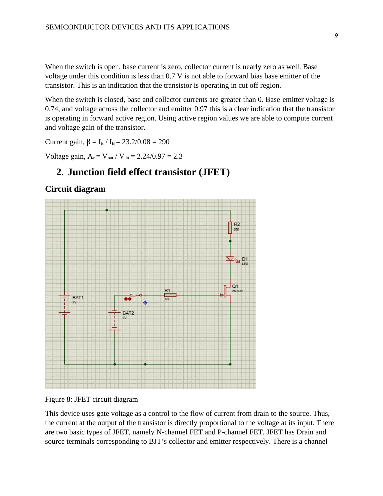
2. Junction field effect transistor (JFET)
Circuit diagram
Figure 8: JFET circuit diagram
This device uses gate voltage as a control to the flow of current from drain to the source. Thus,
the current at the output of the transistor is directly proportional to the voltage at its input. There
are two basic types of JFET, namely N-channel FET and P-channel FET. JFET has Drain and
source terminals corresponding to BJT’s collector and emitter respectively. There is a channel
9
When the switch is open, base current is zero, collector current is nearly zero as well. Base
voltage under this condition is less than 0.7 V is not able to forward bias base emitter of the
transistor. This is an indication that the transistor is operating in cut off region.
When the switch is closed, base and collector currents are greater than 0. Base-emitter voltage is
0.74, and voltage across the collector and emitter 0.97 this is a clear indication that the transistor
is operating in forward active region. Using active region values we are able to compute current
and voltage gain of the transistor.
Current gain, β = IE / IB = 23.2/0.08 = 290
Voltage gain, Av = Vout / V in = 2.24/0.97 = 2.3
2. Junction field effect transistor (JFET)
Circuit diagram
Figure 8: JFET circuit diagram
This device uses gate voltage as a control to the flow of current from drain to the source. Thus,
the current at the output of the transistor is directly proportional to the voltage at its input. There
are two basic types of JFET, namely N-channel FET and P-channel FET. JFET has Drain and
source terminals corresponding to BJT’s collector and emitter respectively. There is a channel
⊘ This is a preview!⊘
Do you want full access?
Subscribe today to unlock all pages.
Trusted by 1+ million students worldwide
SEMICONDUCTOR DEVICES AND ITS APPLICATIONS
10
between the drain and the source that is made up of P-type or N-type material. In N-channel
JFET gate voltage should a negative value whereas that of P-channel should a positive voltage
value.
JFET has depletion layer around the gates which affect the flow of current when its width
changes. When the gate of the transistor is not supplied with any voltage, and a voltage across
the drain and the source is applied, a current will be able to flow through the channel. When
small negative voltage is supplied at the gate of the JFET, the depletion region increases and this
will in turn reduce current that flows through the channel as the effective area of the channel
have been reduced.
When the voltage to the gate is made more negative, the width of depletion layer is increased
further, until flow of current through the channel is no more. when current is no more flowing,
the semiconductor device is said to be pinched off, pinch off is equivalent to cut off region of
BJT.
BJT differs from JFET in that, gate current is zero when the junction is reversed biased and as
for BJT, the junction is reversed biased when base current has a value greater than zero. For
JFET, pinch off occurs at a more negative value and as for BJT, cut off occurs when base current
is zero.
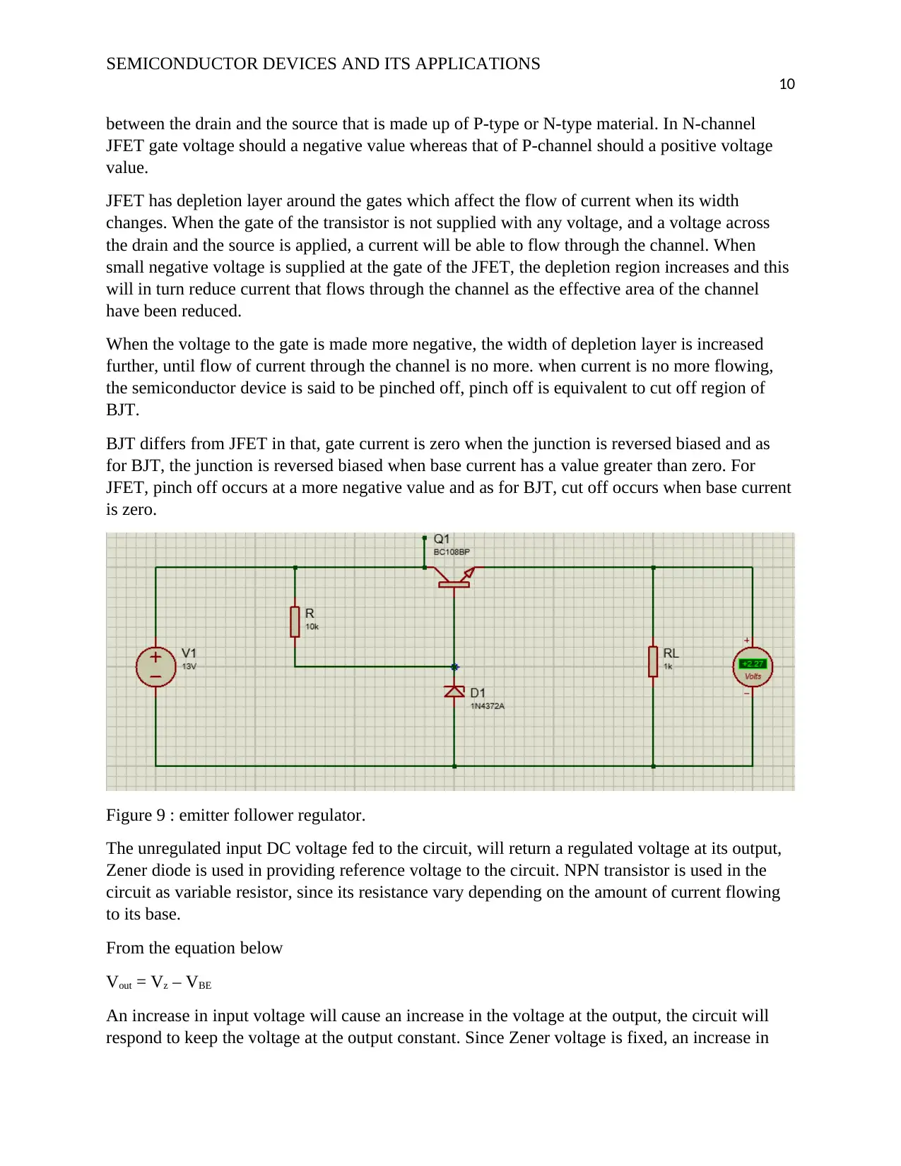
Figure 9 : emitter follower regulator.
The unregulated input DC voltage fed to the circuit, will return a regulated voltage at its output,
Zener diode is used in providing reference voltage to the circuit. NPN transistor is used in the
circuit as variable resistor, since its resistance vary depending on the amount of current flowing
to its base.
From the equation below
Vout = Vz – VBE
An increase in input voltage will cause an increase in the voltage at the output, the circuit will
respond to keep the voltage at the output constant. Since Zener voltage is fixed, an increase in
10
between the drain and the source that is made up of P-type or N-type material. In N-channel
JFET gate voltage should a negative value whereas that of P-channel should a positive voltage
value.
JFET has depletion layer around the gates which affect the flow of current when its width
changes. When the gate of the transistor is not supplied with any voltage, and a voltage across
the drain and the source is applied, a current will be able to flow through the channel. When
small negative voltage is supplied at the gate of the JFET, the depletion region increases and this
will in turn reduce current that flows through the channel as the effective area of the channel
have been reduced.
When the voltage to the gate is made more negative, the width of depletion layer is increased
further, until flow of current through the channel is no more. when current is no more flowing,
the semiconductor device is said to be pinched off, pinch off is equivalent to cut off region of
BJT.
BJT differs from JFET in that, gate current is zero when the junction is reversed biased and as
for BJT, the junction is reversed biased when base current has a value greater than zero. For
JFET, pinch off occurs at a more negative value and as for BJT, cut off occurs when base current
is zero.
Figure 9 : emitter follower regulator.
The unregulated input DC voltage fed to the circuit, will return a regulated voltage at its output,
Zener diode is used in providing reference voltage to the circuit. NPN transistor is used in the
circuit as variable resistor, since its resistance vary depending on the amount of current flowing
to its base.
From the equation below
Vout = Vz – VBE
An increase in input voltage will cause an increase in the voltage at the output, the circuit will
respond to keep the voltage at the output constant. Since Zener voltage is fixed, an increase in
Paraphrase This Document
Need a fresh take? Get an instant paraphrase of this document with our AI Paraphraser
SEMICONDUCTOR DEVICES AND ITS APPLICATIONS
11
the voltage at the output will result to a decrease in voltage across the base of the transistor. This
decrease in the voltage will result to a reduction in a flow of current. Reduced current flow will
cause an increase in voltage across the collector and the emitter and in return voltage at the
output is decreased, compensating for increased voltage. The vice versa applies for decrease in
input voltage
CONCLUSION
Applications of various semi-conductor devices were investigated in the experiment. Regions of
operations of both JFET and BJT regarding its application in switching of devices. Operation of
commonly used voltage regulators specifically emitter follower was discussed. The objectives of
the experiment were met.
SEMICONDUCTOR DEVICES AND ITS APPLICATIONS
12
REFERENCES
Britannica. (n.d). Semiconductor device. Retrieved from
https://www.britannica.com/technology/semiconductor-device/The-p-i-n-diode
ElectronicsTutorial. (n.d). Bipolar transistors. Retrieved from
https://www.electronics-tutorials.ws/transistor/tran_1.html
Elprocus. (n.d). semiconductor devices and circuits, applications. Retrieved from
https://www.elprocus.com/semiconductor-devices-types-and-applications/
Circuit globe. (n.d). NPN Transistor. Retrieved from https://circuitglobe.com/npn-transistor.html
DiMarino, C. M., Burgos, R., & Dushan, B. (2015). High-temperature silicon carbide: characterization
of state-of-the-art silicon carbide power transistors. IEEE Industrial Electronics Magazine, 9(3),
19-30.
Nawaz, M., Chen, N., Chimento, F., & Wang, L. (2016). Static and dynamic characterization of high
power silicon carbide BJT modules. IEEE Transactions on Industry Applications, 52(6), 4990-
4998.
Zhu, H., Sweet, M. R., & Narayanan, E. S. (2015, June). A Comparison of Switching Characteristics
between SiC BJT and Si IGBT at Junction Temperature above 200oC. In PCIM Asia 2015;
International Exhibition and Conference for Power Electronics, Intelligent Motion, Renewable
Energy and Energy Management (pp. 1-8). VDE.
⊘ This is a preview!⊘
Do you want full access?
Subscribe today to unlock all pages.
Trusted by 1+ million students worldwide
1 out of 12
Related Documents


Your All-in-One AI-Powered Toolkit for Academic Success.
+13062052269
info@desklib.com
Available 24*7 on WhatsApp / Email
![[object Object]](/_next/static/media/star-bottom.7253800d.svg)
Unlock your academic potential
Copyright © 2020–2026 A2Z Services. All Rights Reserved. Developed and managed by ZUCOL.