Comprehensive Analysis of Small Signal Amplifier Circuits (US03CPHY22)
VerifiedAdded on 2021/08/30
|19
|4202
|122
Report
AI Summary
This report delves into the analysis of small signal amplifiers, a crucial component in almost all electronic systems. It begins with an introduction to single-stage transistor amplifiers, explaining the role of components like coupling and bypass capacitors. The report then explores two primary methods for analyzing amplifier performance: the graphical method, which utilizes transistor output characteristics, and the equivalent circuit method, which simplifies the circuit for AC analysis. The graphical method includes the concept of DC and AC load lines, while the equivalent circuit method introduces the h-parameter equivalent circuit. The document covers the calculation of voltage and current gain using the graphical method and discusses the phase relationships between input and output signals. Finally, it presents the development and application of the h-parameter equivalent circuit for comprehensive amplifier analysis.
Physics Department Bhrijesh N Patel
1 | P a g e
Shree P M Patel College of Electronics and Communication, Anand
S.Y. B.Sc. Semester - III
US03CPHY22 Basic Solid State Electronics
Unit – 2 Small Signal Amplifier
Introduction
Almost no electronic system can work without an amplifier. It is only
because of the enlargement or the amplification of the signal picked up by
microphone that we can enjoy a music orchestra. We are able to hear the
news or the cricket commentary on our radio, simply because the amplifier
in the radio amplifies the weak signals received by its antenna. The signal
can only be of any use if it is amplified to give a suitable output.
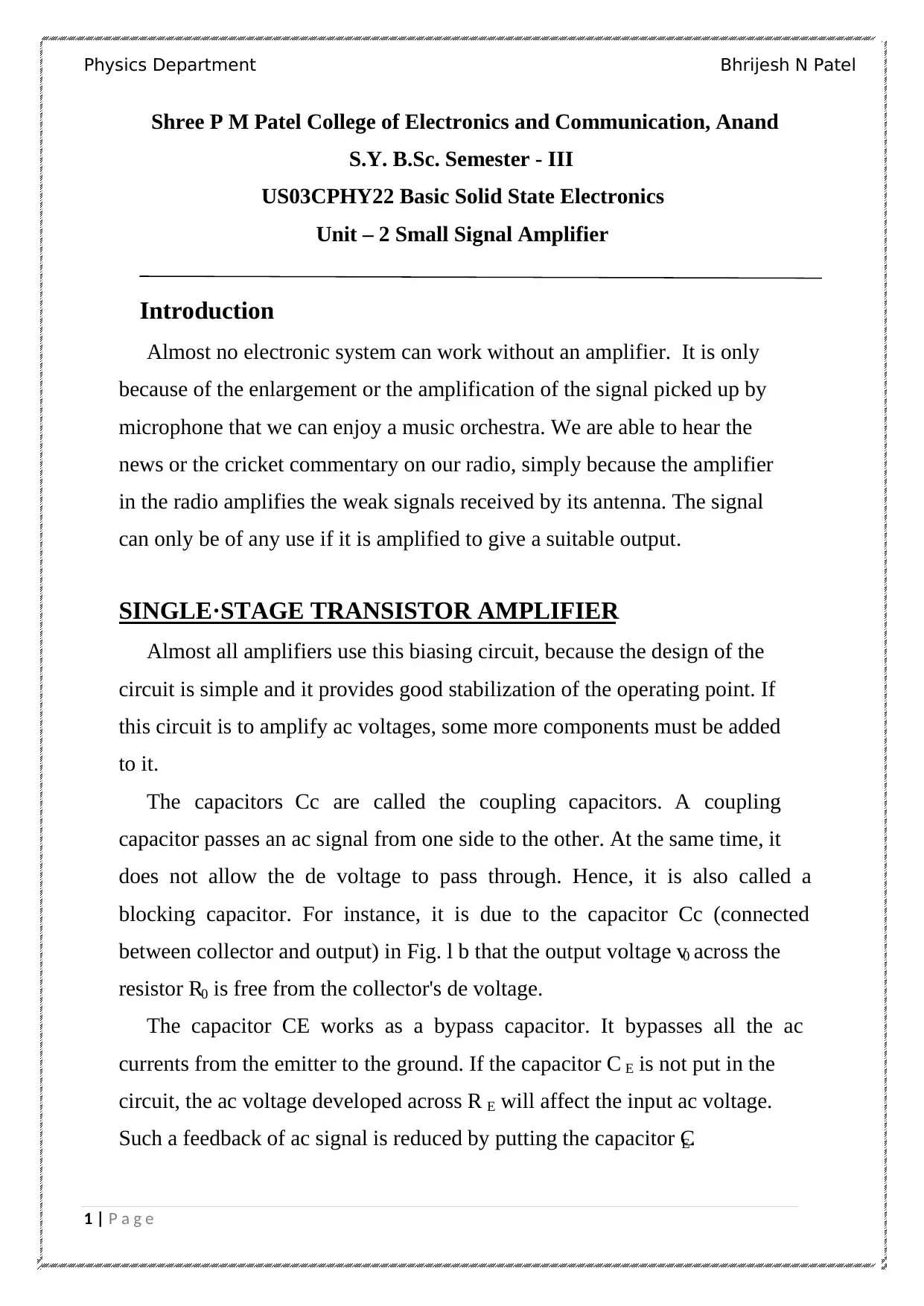
SINGLE·STAGE TRANSISTOR AMPLIFIER
Almost all amplifiers use this biasing circuit, because the design of the
circuit is simple and it provides good stabilization of the operating point. If
this circuit is to amplify ac voltages, some more components must be added
to it.
The capacitors Cc are called the coupling capacitors. A coupling
capacitor passes an ac signal from one side to the other. At the same time, it
does not allow the de voltage to pass through. Hence, it is also called a
blocking capacitor. For instance, it is due to the capacitor Cc (connected
between collector and output) in Fig. l b that the output voltage v0 across the
resistor R0 is free from the collector's de voltage.
The capacitor CE works as a bypass capacitor. It bypasses all the ac
currents from the emitter to the ground. If the capacitor C E is not put in the
circuit, the ac voltage developed across R E will affect the input ac voltage.
Such a feedback of ac signal is reduced by putting the capacitor CE.
1 | P a g e
Shree P M Patel College of Electronics and Communication, Anand
S.Y. B.Sc. Semester - III
US03CPHY22 Basic Solid State Electronics
Unit – 2 Small Signal Amplifier
Introduction
Almost no electronic system can work without an amplifier. It is only
because of the enlargement or the amplification of the signal picked up by
microphone that we can enjoy a music orchestra. We are able to hear the
news or the cricket commentary on our radio, simply because the amplifier
in the radio amplifies the weak signals received by its antenna. The signal
can only be of any use if it is amplified to give a suitable output.
SINGLE·STAGE TRANSISTOR AMPLIFIER
Almost all amplifiers use this biasing circuit, because the design of the
circuit is simple and it provides good stabilization of the operating point. If
this circuit is to amplify ac voltages, some more components must be added
to it.
The capacitors Cc are called the coupling capacitors. A coupling
capacitor passes an ac signal from one side to the other. At the same time, it
does not allow the de voltage to pass through. Hence, it is also called a
blocking capacitor. For instance, it is due to the capacitor Cc (connected
between collector and output) in Fig. l b that the output voltage v0 across the
resistor R0 is free from the collector's de voltage.
The capacitor CE works as a bypass capacitor. It bypasses all the ac
currents from the emitter to the ground. If the capacitor C E is not put in the
circuit, the ac voltage developed across R E will affect the input ac voltage.
Such a feedback of ac signal is reduced by putting the capacitor CE.
Paraphrase This Document
Need a fresh take? Get an instant paraphrase of this document with our AI Paraphraser
Physics Department Bhrijesh N Patel
2 | P a g e
(a) Voltage-divider biasing circuit (b) same circuit converted into an amplifier
If the capacitor CE is good enough to provide an effective bypass to the
lowest frequency of the signal, it will do so better to the higher frequencies.
We, therefore, select such a value of capacitor CE that gives quite a low
impedance compared to RE at the lowest frequency present in the input
signal.
To what extent an amplifier enlarges signals is expressed in terms of its
voltage gain. The voltage gain of an amplifier is given as
The other quantities of interest for a voltage amplifier are its current gain
(Ai), input impedance (Zi), and output impedance (Z0). The amplifier can be
analysed for its performance by the following two methods:
1. Graphical method
2. Equivalent circuit method
Physics Department Bhrijesh N Patel
3 | P a g e
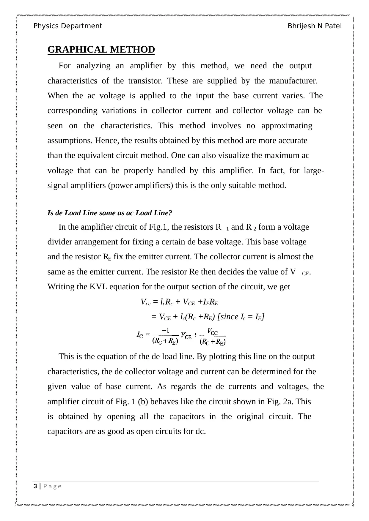
GRAPHICAL METHOD
For analyzing an amplifier by this method, we need the output
characteristics of the transistor. These are supplied by the manufacturer.
When the ac voltage is applied to the input the base current varies. The
corresponding variations in collector current and collector voltage can be
seen on the characteristics. This method involves no approximating
assumptions. Hence, the results obtained by this method are more accurate
than the equivalent circuit method. One can also visualize the maximum ac
voltage that can be properly handled by this amplifier. In fact, for large-
signal amplifiers (power amplifiers) this is the only suitable method.
Is de Load Line same as ac Load Line?
In the amplifier circuit of Fig.1, the resistors R 1 and R 2 form a voltage
divider arrangement for fixing a certain de base voltage. This base voltage
and the resistor RE fix the emitter current. The collector current is almost the
same as the emitter current. The resistor Re then decides the value of V CE.
Writing the KVL equation for the output section of the circuit, we get
Vcc = lcRc + VCE +IERE
= VCE + lc(Rc +RE) [since Ic = IE]
This is the equation of the de load line. By plotting this line on the output
characteristics, the de collector voltage and current can be determined for the
given value of base current. As regards the de currents and voltages, the
amplifier circuit of Fig. 1 (b) behaves like the circuit shown in Fig. 2a. This
is obtained by opening all the capacitors in the original circuit. The
capacitors are as good as open circuits for dc.
3 | P a g e
GRAPHICAL METHOD
For analyzing an amplifier by this method, we need the output
characteristics of the transistor. These are supplied by the manufacturer.
When the ac voltage is applied to the input the base current varies. The
corresponding variations in collector current and collector voltage can be
seen on the characteristics. This method involves no approximating
assumptions. Hence, the results obtained by this method are more accurate
than the equivalent circuit method. One can also visualize the maximum ac
voltage that can be properly handled by this amplifier. In fact, for large-
signal amplifiers (power amplifiers) this is the only suitable method.
Is de Load Line same as ac Load Line?
In the amplifier circuit of Fig.1, the resistors R 1 and R 2 form a voltage
divider arrangement for fixing a certain de base voltage. This base voltage
and the resistor RE fix the emitter current. The collector current is almost the
same as the emitter current. The resistor Re then decides the value of V CE.
Writing the KVL equation for the output section of the circuit, we get
Vcc = lcRc + VCE +IERE
= VCE + lc(Rc +RE) [since Ic = IE]
This is the equation of the de load line. By plotting this line on the output
characteristics, the de collector voltage and current can be determined for the
given value of base current. As regards the de currents and voltages, the
amplifier circuit of Fig. 1 (b) behaves like the circuit shown in Fig. 2a. This
is obtained by opening all the capacitors in the original circuit. The
capacitors are as good as open circuits for dc.
⊘ This is a preview!⊘
Do you want full access?
Subscribe today to unlock all pages.
Trusted by 1+ million students worldwide
Physics Department Bhrijesh N Patel
4 | P a g e
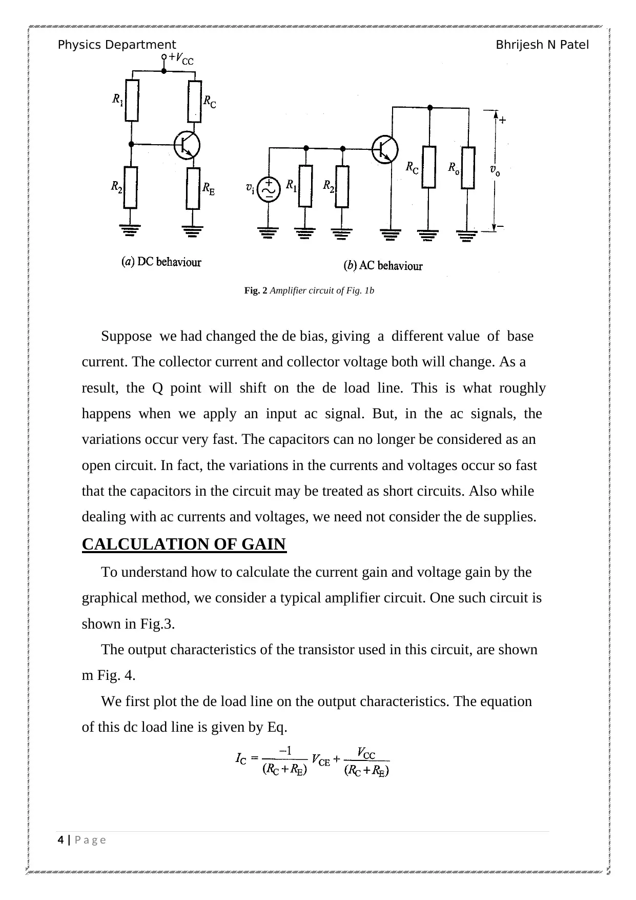
Fig. 2 Amplifier circuit of Fig. 1b
Suppose we had changed the de bias, giving a different value of base
current. The collector current and collector voltage both will change. As a
result, the Q point will shift on the de load line. This is what roughly
happens when we apply an input ac signal. But, in the ac signals, the
variations occur very fast. The capacitors can no longer be considered as an
open circuit. In fact, the variations in the currents and voltages occur so fast
that the capacitors in the circuit may be treated as short circuits. Also while
dealing with ac currents and voltages, we need not consider the de supplies.
CALCULATION OF GAIN
To understand how to calculate the current gain and voltage gain by the
graphical method, we consider a typical amplifier circuit. One such circuit is
shown in Fig.3.
The output characteristics of the transistor used in this circuit, are shown
m Fig. 4.
We first plot the de load line on the output characteristics. The equation
of this dc load line is given by Eq.
4 | P a g e
Fig. 2 Amplifier circuit of Fig. 1b
Suppose we had changed the de bias, giving a different value of base
current. The collector current and collector voltage both will change. As a
result, the Q point will shift on the de load line. This is what roughly
happens when we apply an input ac signal. But, in the ac signals, the
variations occur very fast. The capacitors can no longer be considered as an
open circuit. In fact, the variations in the currents and voltages occur so fast
that the capacitors in the circuit may be treated as short circuits. Also while
dealing with ac currents and voltages, we need not consider the de supplies.
CALCULATION OF GAIN
To understand how to calculate the current gain and voltage gain by the
graphical method, we consider a typical amplifier circuit. One such circuit is
shown in Fig.3.
The output characteristics of the transistor used in this circuit, are shown
m Fig. 4.
We first plot the de load line on the output characteristics. The equation
of this dc load line is given by Eq.
Paraphrase This Document
Need a fresh take? Get an instant paraphrase of this document with our AI Paraphraser
Physics Department Bhrijesh N Patel
5 | P a g e
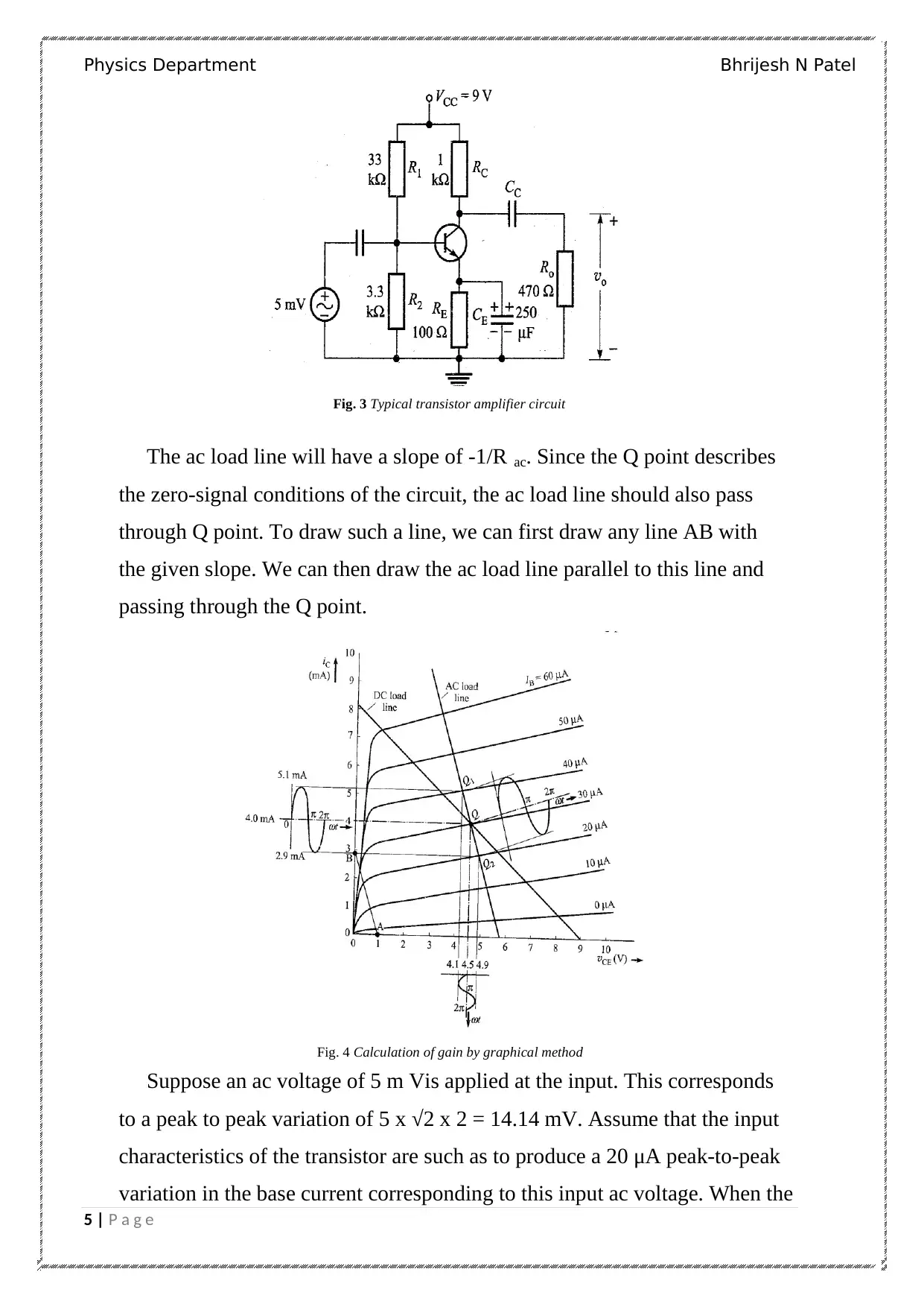
Fig. 3 Typical transistor amplifier circuit
The ac load line will have a slope of -1/R ac. Since the Q point describes
the zero-signal conditions of the circuit, the ac load line should also pass
through Q point. To draw such a line, we can first draw any line AB with
the given slope. We can then draw the ac load line parallel to this line and
passing through the Q point.
Fig. 4 Calculation of gain by graphical method
Suppose an ac voltage of 5 m Vis applied at the input. This corresponds
to a peak to peak variation of 5 x √2 x 2 = 14.14 mV. Assume that the input
characteristics of the transistor are such as to produce a 20 μA peak-to-peak
variation in the base current corresponding to this input ac voltage. When the
5 | P a g e
Fig. 3 Typical transistor amplifier circuit
The ac load line will have a slope of -1/R ac. Since the Q point describes
the zero-signal conditions of the circuit, the ac load line should also pass
through Q point. To draw such a line, we can first draw any line AB with
the given slope. We can then draw the ac load line parallel to this line and
passing through the Q point.
Fig. 4 Calculation of gain by graphical method
Suppose an ac voltage of 5 m Vis applied at the input. This corresponds
to a peak to peak variation of 5 x √2 x 2 = 14.14 mV. Assume that the input
characteristics of the transistor are such as to produce a 20 μA peak-to-peak
variation in the base current corresponding to this input ac voltage. When the
Physics Department Bhrijesh N Patel
6 | P a g e
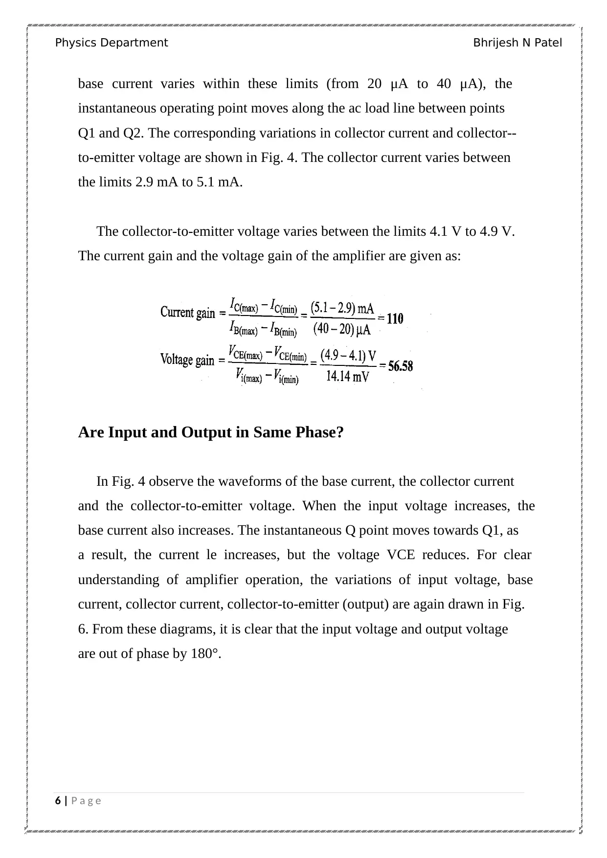
base current varies within these limits (from 20 μA to 40 μA), the
instantaneous operating point moves along the ac load line between points
Q1 and Q2. The corresponding variations in collector current and collector--
to-emitter voltage are shown in Fig. 4. The collector current varies between
the limits 2.9 mA to 5.1 mA.
The collector-to-emitter voltage varies between the limits 4.1 V to 4.9 V.
The current gain and the voltage gain of the amplifier are given as:
Are Input and Output in Same Phase?
In Fig. 4 observe the waveforms of the base current, the collector current
and the collector-to-emitter voltage. When the input voltage increases, the
base current also increases. The instantaneous Q point moves towards Q1, as
a result, the current le increases, but the voltage VCE reduces. For clear
understanding of amplifier operation, the variations of input voltage, base
current, collector current, collector-to-emitter (output) are again drawn in Fig.
6. From these diagrams, it is clear that the input voltage and output voltage
are out of phase by 180°.
6 | P a g e
base current varies within these limits (from 20 μA to 40 μA), the
instantaneous operating point moves along the ac load line between points
Q1 and Q2. The corresponding variations in collector current and collector--
to-emitter voltage are shown in Fig. 4. The collector current varies between
the limits 2.9 mA to 5.1 mA.
The collector-to-emitter voltage varies between the limits 4.1 V to 4.9 V.
The current gain and the voltage gain of the amplifier are given as:
Are Input and Output in Same Phase?
In Fig. 4 observe the waveforms of the base current, the collector current
and the collector-to-emitter voltage. When the input voltage increases, the
base current also increases. The instantaneous Q point moves towards Q1, as
a result, the current le increases, but the voltage VCE reduces. For clear
understanding of amplifier operation, the variations of input voltage, base
current, collector current, collector-to-emitter (output) are again drawn in Fig.
6. From these diagrams, it is clear that the input voltage and output voltage
are out of phase by 180°.
⊘ This is a preview!⊘
Do you want full access?
Subscribe today to unlock all pages.
Trusted by 1+ million students worldwide
Physics Department Bhrijesh N Patel
7 | P a g e
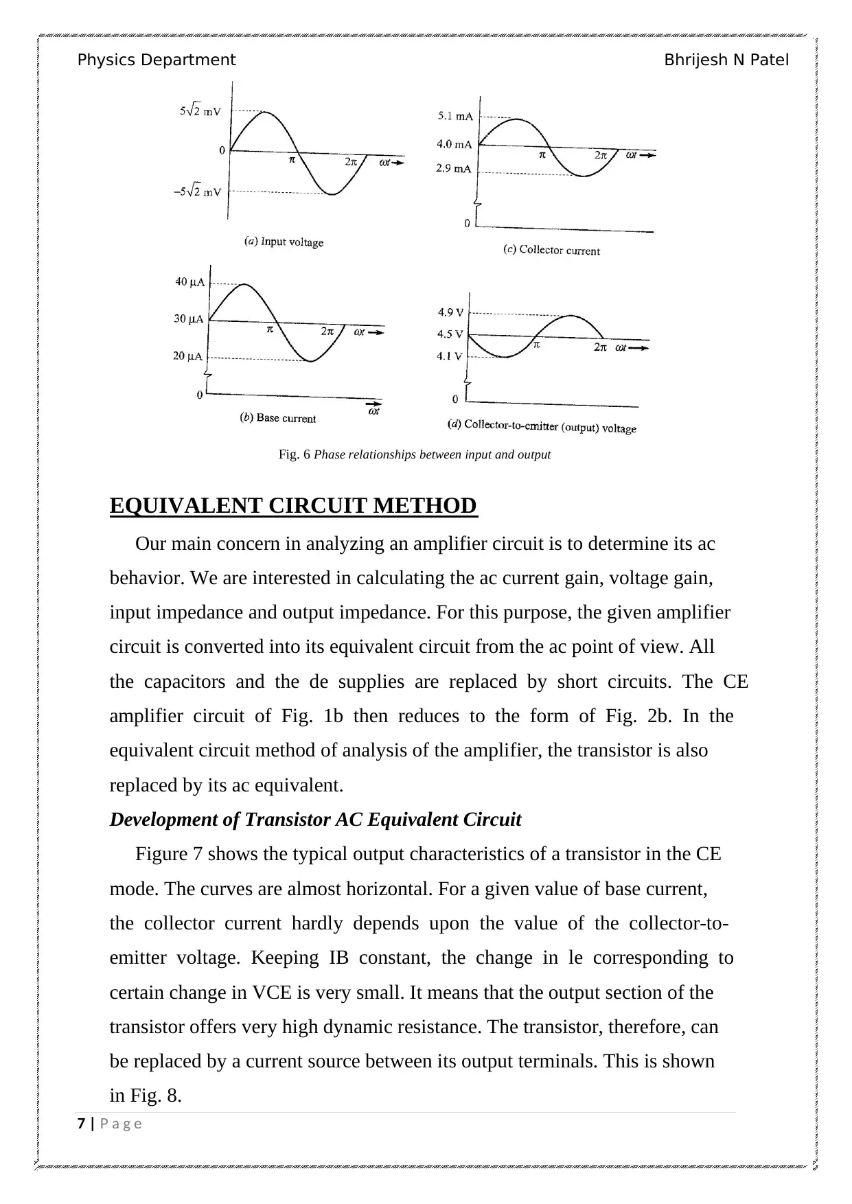
Fig. 6 Phase relationships between input and output
EQUIVALENT CIRCUIT METHOD
Our main concern in analyzing an amplifier circuit is to determine its ac
behavior. We are interested in calculating the ac current gain, voltage gain,
input impedance and output impedance. For this purpose, the given amplifier
circuit is converted into its equivalent circuit from the ac point of view. All
the capacitors and the de supplies are replaced by short circuits. The CE
amplifier circuit of Fig. 1b then reduces to the form of Fig. 2b. In the
equivalent circuit method of analysis of the amplifier, the transistor is also
replaced by its ac equivalent.
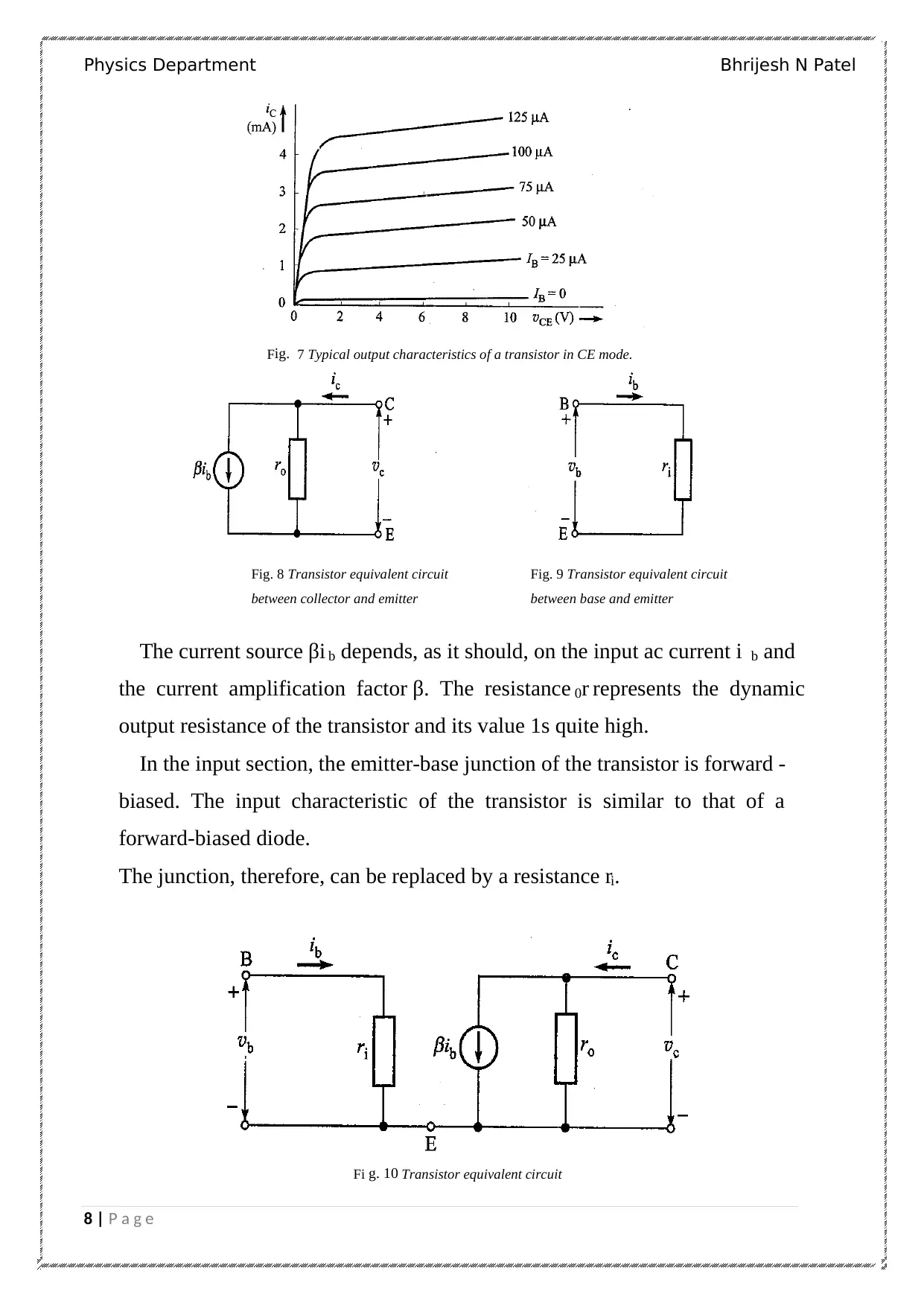
Development of Transistor AC Equivalent Circuit
Figure 7 shows the typical output characteristics of a transistor in the CE
mode. The curves are almost horizontal. For a given value of base current,
the collector current hardly depends upon the value of the collector-to-
emitter voltage. Keeping IB constant, the change in le corresponding to
certain change in VCE is very small. It means that the output section of the
transistor offers very high dynamic resistance. The transistor, therefore, can
be replaced by a current source between its output terminals. This is shown
in Fig. 8.
7 | P a g e
Fig. 6 Phase relationships between input and output
EQUIVALENT CIRCUIT METHOD
Our main concern in analyzing an amplifier circuit is to determine its ac
behavior. We are interested in calculating the ac current gain, voltage gain,
input impedance and output impedance. For this purpose, the given amplifier
circuit is converted into its equivalent circuit from the ac point of view. All
the capacitors and the de supplies are replaced by short circuits. The CE
amplifier circuit of Fig. 1b then reduces to the form of Fig. 2b. In the
equivalent circuit method of analysis of the amplifier, the transistor is also
replaced by its ac equivalent.
Development of Transistor AC Equivalent Circuit
Figure 7 shows the typical output characteristics of a transistor in the CE
mode. The curves are almost horizontal. For a given value of base current,
the collector current hardly depends upon the value of the collector-to-
emitter voltage. Keeping IB constant, the change in le corresponding to
certain change in VCE is very small. It means that the output section of the
transistor offers very high dynamic resistance. The transistor, therefore, can
be replaced by a current source between its output terminals. This is shown
in Fig. 8.
Paraphrase This Document
Need a fresh take? Get an instant paraphrase of this document with our AI Paraphraser
Physics Department Bhrijesh N Patel
8 | P a g e
Fig. 7 Typical output characteristics of a transistor in CE mode.
Fig. 8 Transistor equivalent circuit Fig. 9 Transistor equivalent circuit
between collector and emitter between base and emitter
The current source βi b depends, as it should, on the input ac current i b and
the current amplification factor β. The resistance r0 represents the dynamic
output resistance of the transistor and its value 1s quite high.
In the input section, the emitter-base junction of the transistor is forward -
biased. The input characteristic of the transistor is similar to that of a
forward-biased diode.
The junction, therefore, can be replaced by a resistance ri.
Fi g. 10 Transistor equivalent circuit
Physics Department Bhrijesh N Patel
9 | P a g e
h-parameter Equivalent Circuit
Quite often, the manufacturers specify the characteristics of a transistor in
terms of its h parameters (the letter h stands for hybrid). The word hybrid is
used with these parameters because they are a mixture of constants having
different units. The hybrid parameters have become popular because they can
be measured easily.
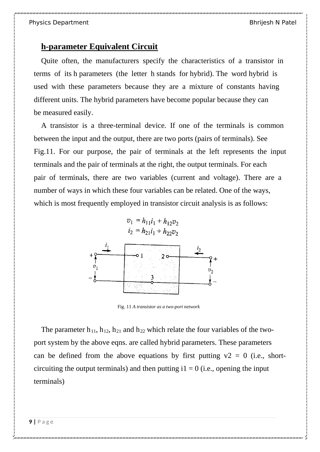
A transistor is a three-terminal device. If one of the terminals is common
between the input and the output, there are two ports (pairs of terminals). See
Fig.11. For our purpose, the pair of terminals at the left represents the input
terminals and the pair of terminals at the right, the output terminals. For each
pair of terminals, there are two variables (current and voltage). There are a
number of ways in which these four variables can be related. One of the ways,
which is most frequently employed in transistor circuit analysis is as follows:
Fig. 11 A transistor as a two-port network
The parameter h11, h12, h21 and h22 which relate the four variables of the two-
port system by the above eqns. are called hybrid parameters. These parameters
can be defined from the above equations by first putting v2 = 0 (i.e., short-
circuiting the output terminals) and then putting i1 = 0 (i.e., opening the input
terminals)
9 | P a g e
h-parameter Equivalent Circuit
Quite often, the manufacturers specify the characteristics of a transistor in
terms of its h parameters (the letter h stands for hybrid). The word hybrid is
used with these parameters because they are a mixture of constants having
different units. The hybrid parameters have become popular because they can
be measured easily.
A transistor is a three-terminal device. If one of the terminals is common
between the input and the output, there are two ports (pairs of terminals). See
Fig.11. For our purpose, the pair of terminals at the left represents the input
terminals and the pair of terminals at the right, the output terminals. For each
pair of terminals, there are two variables (current and voltage). There are a
number of ways in which these four variables can be related. One of the ways,
which is most frequently employed in transistor circuit analysis is as follows:
Fig. 11 A transistor as a two-port network
The parameter h11, h12, h21 and h22 which relate the four variables of the two-
port system by the above eqns. are called hybrid parameters. These parameters
can be defined from the above equations by first putting v2 = 0 (i.e., short-
circuiting the output terminals) and then putting i1 = 0 (i.e., opening the input
terminals)
⊘ This is a preview!⊘
Do you want full access?
Subscribe today to unlock all pages.
Trusted by 1+ million students worldwide
Physics Department Bhrijesh N Patel
10 | P a g e
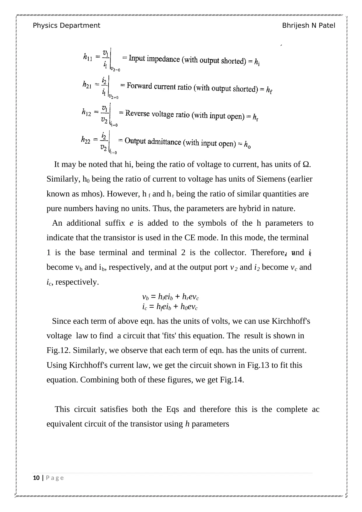
It may be noted that hi, being the ratio of voltage to current, has units of Ω.
Similarly, h0 being the ratio of current to voltage has units of Siemens (earlier
known as mhos). However, h f and h r being the ratio of similar quantities are
pure numbers having no units. Thus, the parameters are hybrid in nature.
An additional suffix e is added to the symbols of the h parameters to
indicate that the transistor is used in the CE mode. In this mode, the terminal
1 is the base terminal and terminal 2 is the collector. Therefore, v1 and i1
become vb and ib, respectively, and at the output port v 2 and i2 become vc and
ic, respectively.
vb = hieib + hrevc
ic = hfeib + h0evc
Since each term of above eqn. has the units of volts, we can use Kirchhoff's
voltage law to find a circuit that 'fits' this equation. The result is shown in
Fig.12. Similarly, we observe that each term of eqn. has the units of current.
Using Kirchhoff's current law, we get the circuit shown in Fig.13 to fit this
equation. Combining both of these figures, we get Fig.14.
This circuit satisfies both the Eqs and therefore this is the complete ac
equivalent circuit of the transistor using h parameters.
10 | P a g e
It may be noted that hi, being the ratio of voltage to current, has units of Ω.
Similarly, h0 being the ratio of current to voltage has units of Siemens (earlier
known as mhos). However, h f and h r being the ratio of similar quantities are
pure numbers having no units. Thus, the parameters are hybrid in nature.
An additional suffix e is added to the symbols of the h parameters to
indicate that the transistor is used in the CE mode. In this mode, the terminal
1 is the base terminal and terminal 2 is the collector. Therefore, v1 and i1
become vb and ib, respectively, and at the output port v 2 and i2 become vc and
ic, respectively.
vb = hieib + hrevc
ic = hfeib + h0evc
Since each term of above eqn. has the units of volts, we can use Kirchhoff's
voltage law to find a circuit that 'fits' this equation. The result is shown in
Fig.12. Similarly, we observe that each term of eqn. has the units of current.
Using Kirchhoff's current law, we get the circuit shown in Fig.13 to fit this
equation. Combining both of these figures, we get Fig.14.
This circuit satisfies both the Eqs and therefore this is the complete ac
equivalent circuit of the transistor using h parameters.
Paraphrase This Document
Need a fresh take? Get an instant paraphrase of this document with our AI Paraphraser
Physics Department Bhrijesh N Patel
11 | P a g e
Fig. 12 Hybrid input equivalent circuit Fig. 13 Hybrid output equivalent circuit
Fig. 14 Complete hybrid equivalent circuit of a transistor
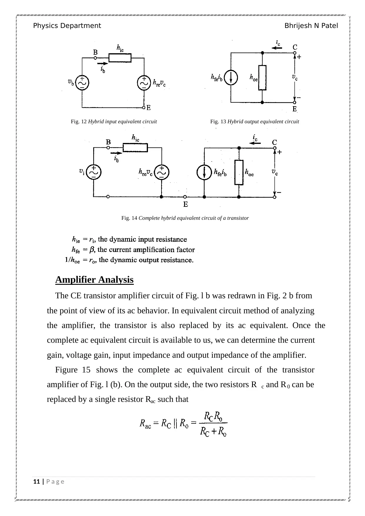
Amplifier Analysis
The CE transistor amplifier circuit of Fig. l b was redrawn in Fig. 2 b from
the point of view of its ac behavior. In equivalent circuit method of analyzing
the amplifier, the transistor is also replaced by its ac equivalent. Once the
complete ac equivalent circuit is available to us, we can determine the current
gain, voltage gain, input impedance and output impedance of the amplifier.
Figure 15 shows the complete ac equivalent circuit of the transistor
amplifier of Fig. l (b). On the output side, the two resistors R c and R0 can be
replaced by a single resistor Rac such that
11 | P a g e
Fig. 12 Hybrid input equivalent circuit Fig. 13 Hybrid output equivalent circuit
Fig. 14 Complete hybrid equivalent circuit of a transistor
Amplifier Analysis
The CE transistor amplifier circuit of Fig. l b was redrawn in Fig. 2 b from
the point of view of its ac behavior. In equivalent circuit method of analyzing
the amplifier, the transistor is also replaced by its ac equivalent. Once the
complete ac equivalent circuit is available to us, we can determine the current
gain, voltage gain, input impedance and output impedance of the amplifier.
Figure 15 shows the complete ac equivalent circuit of the transistor
amplifier of Fig. l (b). On the output side, the two resistors R c and R0 can be
replaced by a single resistor Rac such that
Physics Department Bhrijesh N Patel
12 | P a g e
Fig. 15 Complete ac equivalent circuit of the transistor amplifier
On the input side, if the input voltage source vi is assumed to be ideal (with
zero internal resistance), the presence or the absence of the resistors R 1 and
R2 is immaterial. Whatever may be the values of R1 and R2 the current ib
remains the same. We can therefore ignore these resistors altogether. The
result is the circuit of Fig.16.
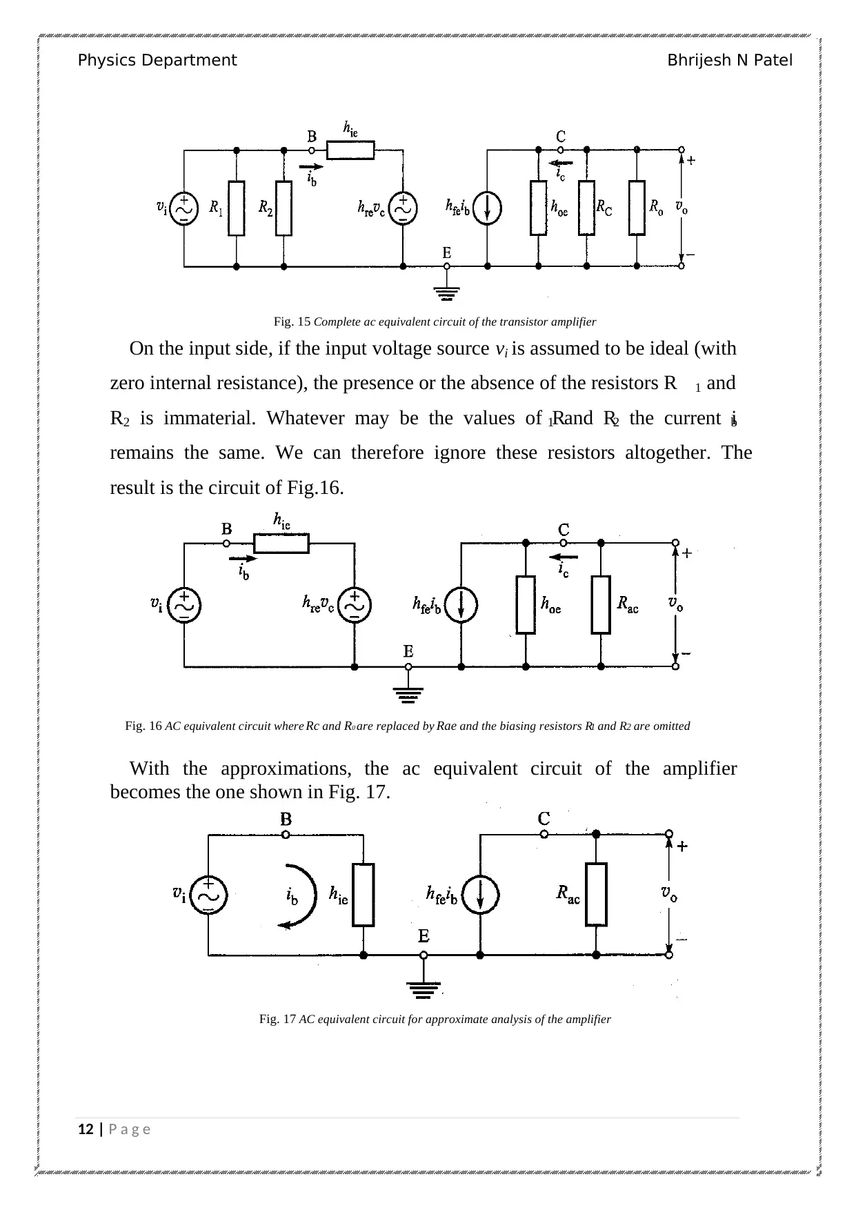
Fig. 16 AC equivalent circuit where Rc and R0 are replaced by Rae and the biasing resistors R1 and R2 are omitted
With the approximations, the ac equivalent circuit of the amplifier
becomes the one shown in Fig. 17.
Fig. 17 AC equivalent circuit for approximate analysis of the amplifier
12 | P a g e
Fig. 15 Complete ac equivalent circuit of the transistor amplifier
On the input side, if the input voltage source vi is assumed to be ideal (with
zero internal resistance), the presence or the absence of the resistors R 1 and
R2 is immaterial. Whatever may be the values of R1 and R2 the current ib
remains the same. We can therefore ignore these resistors altogether. The
result is the circuit of Fig.16.
Fig. 16 AC equivalent circuit where Rc and R0 are replaced by Rae and the biasing resistors R1 and R2 are omitted
With the approximations, the ac equivalent circuit of the amplifier
becomes the one shown in Fig. 17.
Fig. 17 AC equivalent circuit for approximate analysis of the amplifier
⊘ This is a preview!⊘
Do you want full access?
Subscribe today to unlock all pages.
Trusted by 1+ million students worldwide
1 out of 19
Related Documents


Your All-in-One AI-Powered Toolkit for Academic Success.
+13062052269
info@desklib.com
Available 24*7 on WhatsApp / Email
![[object Object]](/_next/static/media/star-bottom.7253800d.svg)
Unlock your academic potential
Copyright © 2020–2026 A2Z Services. All Rights Reserved. Developed and managed by ZUCOL.