VHDL Register File: Structural Design, Implementation & Testing

Verified

Added on  2023/04/20

|4
|928
|211
Practical Assignment
AI Summary
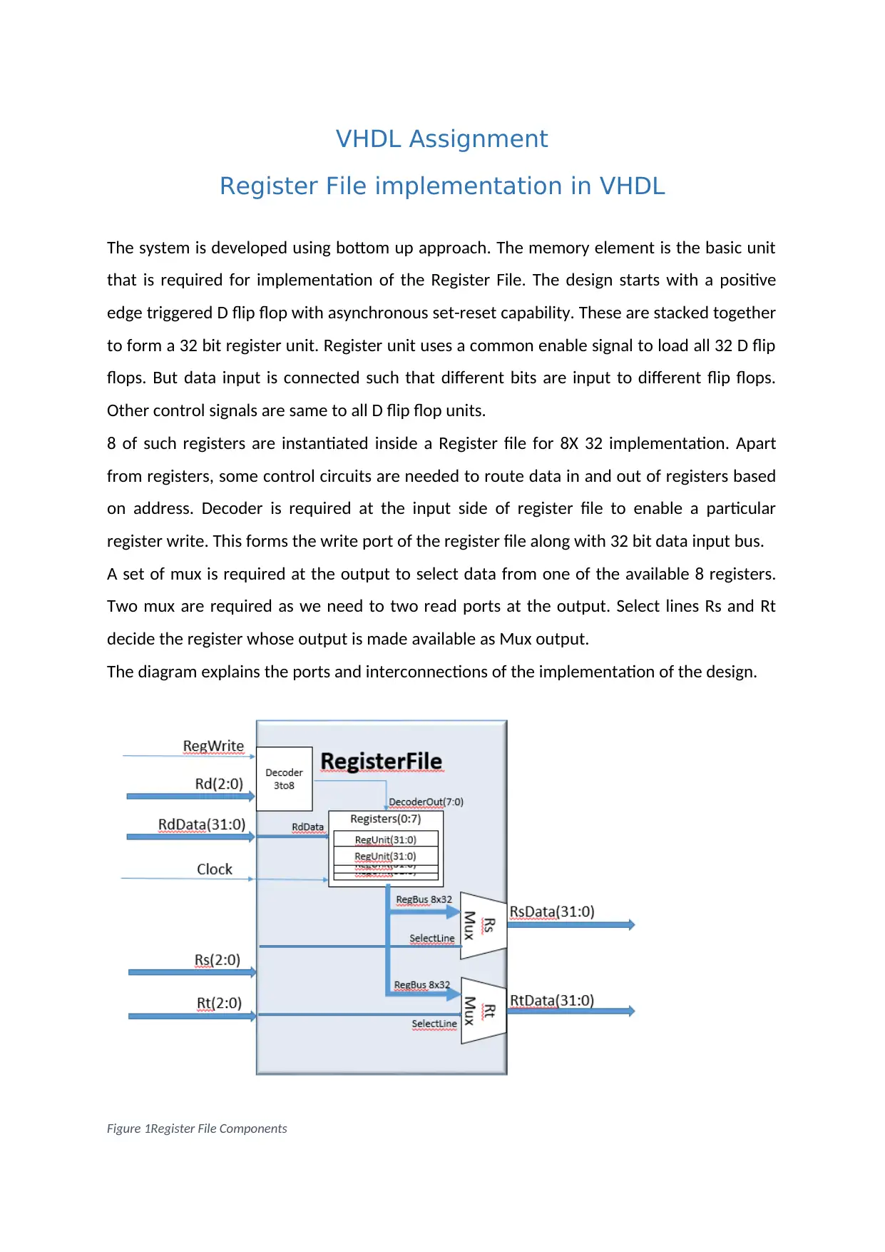
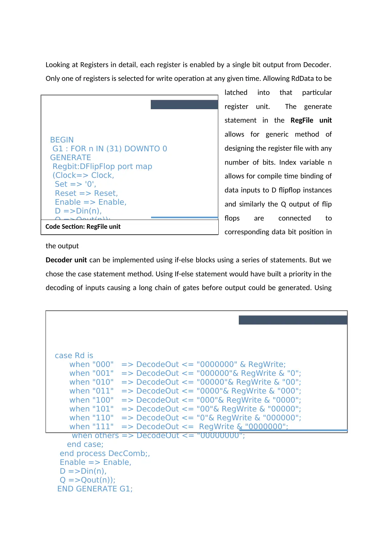
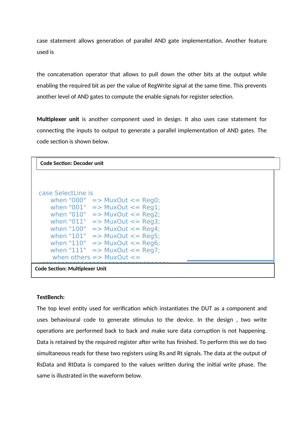
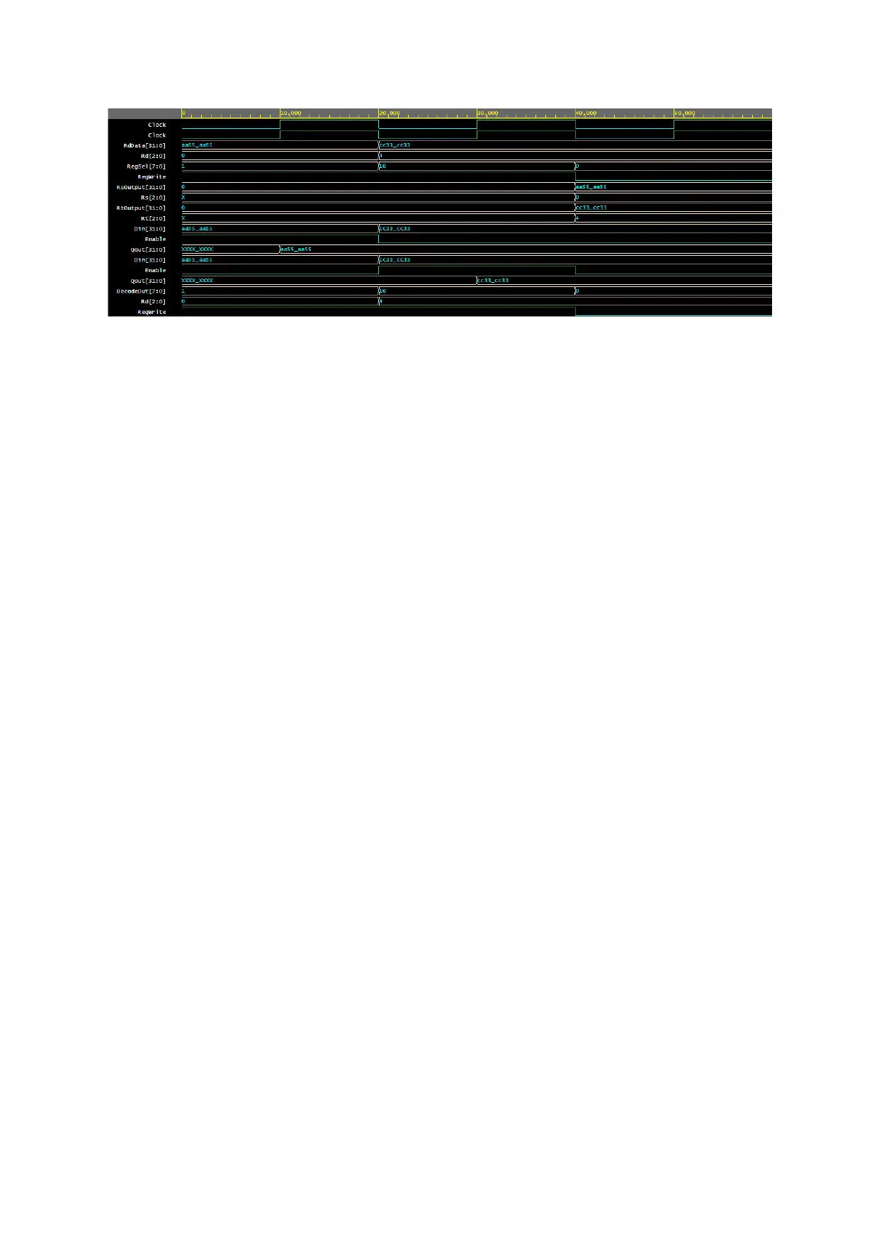
This assignment solution provides a detailed implementation of an 8x32 register file in VHDL using structural modeling. The design utilizes a bottom-up approach, starting with a positive edge-triggered D flip-flop as the basic memory element. These flip-flops are combined to form a 32-bit register unit, which are then instantiated eight times within the register file. The design incorporates a decoder for register write selection and multiplexers for implementing two read ports. The solution includes VHDL code for the D flip-flop, register unit, decoder, multiplexer, and the top-level register file entity. A testbench is also provided to verify the functionality of the register file, ensuring data integrity during simultaneous read and write operations. The testbench performs back-to-back write operations and verifies data retention through simultaneous reads, demonstrating the correct operation of the register file.
Document Page
VHDL Assignment
Register File implementation in VHDL
The system is developed using bottom up approach. The memory element is the basic unit
that is required for implementation of the Register File. The design starts with a positive
edge triggered D flip flop with asynchronous set-reset capability. These are stacked together
to form a 32 bit register unit. Register unit uses a common enable signal to load all 32 D flip
flops. But data input is connected such that different bits are input to different flip flops.
Other control signals are same to all D flip flop units.
8 of such registers are instantiated inside a Register file for 8X 32 implementation. Apart
from registers, some control circuits are needed to route data in and out of registers based
on address. Decoder is required at the input side of register file to enable a particular
register write. This forms the write port of the register file along with 32 bit data input bus.
A set of mux is required at the output to select data from one of the available 8 registers.
Two mux are required as we need to two read ports at the output. Select lines Rs and Rt
decide the register whose output is made available as Mux output.
The diagram explains the ports and interconnections of the implementation of the design.
Figure 1Register File Components
tabler-icon-diamond-filled.svg

Paraphrase This Document

Need a fresh take? Get an instant paraphrase of this document with our AI Paraphraser
Document Page
Looking at Registers in detail, each register is enabled by a single bit output from Decoder.
Only one of registers is selected for write operation at any given time. Allowing RdData to be
latched into that particular
register unit. The generate
statement in the RegFile unit
allows for generic method of
designing the register file with any
number of bits. Index variable n
allows for compile time binding of
data inputs to D flipflop instances
and similarly the Q output of flip
flops are connected to
corresponding data bit position in
the output
Decoder unit can be implemented using if-else blocks using a series of statements. But we
chose the case statement method. Using If-else statement would have built a priority in the
decoding of inputs causing a long chain of gates before output could be generated. Using
BEGIN
G1 : FOR n IN (31) DOWNTO 0
GENERATE
Regbit:DFlipFlop port map
(Clock=> Clock,
Set => '0',
Reset => Reset,
Enable => Enable,
D =>Din(n),
Q =>Qout(n));
END GENERATE G1;
case Rd is
when "000" => DecodeOut <= "0000000" & RegWrite;
when "001" => DecodeOut <= "000000"& RegWrite & "0";
when "010" => DecodeOut <= "00000"& RegWrite & "00";
when "011" => DecodeOut <= "0000"& RegWrite & "000";
when "100" => DecodeOut <= "000"& RegWrite & "0000";
when "101" => DecodeOut <= "00"& RegWrite & "00000";
when "110" => DecodeOut <= "0"& RegWrite & "000000";
when "111" => DecodeOut <= RegWrite & "0000000";
when others => DecodeOut <= "00000000";
end case;
end process DecComb;,
Enable => Enable,
D =>Din(n),
Q =>Qout(n));
END GENERATE G1;
Code Section: RegFile unit
Document Page
case statement allows generation of parallel AND gate implementation. Another feature
used is
the concatenation operator that allows to pull down the other bits at the output while
enabling the required bit as per the value of RegWrite signal at the same time. This prevents
another level of AND gates to compute the enable signals for register selection.
Multiplexer unit is another component used in design. It also uses case statement for
connecting the inputs to output to generate a parallel implementation of AND gates. The
code section is shown below.
TestBench:
The top level entity used for verification which instantiates the DUT as a component and
uses behavioural code to generate stimulus to the device. In the design , two write
operations are performed back to back and make sure data corruption is not happening.
Data is retained by the required register after write has finished. To perform this we do two
simultaneous reads for these two registers using Rs and Rt signals. The data at the output of
RsData and RtData is compared to the values written during the initial write phase. The
same is illustrated in the waveform below.
case SelectLine is
when "000" => MuxOut <= Reg0;
when "001" => MuxOut <= Reg1;
when "010" => MuxOut <= Reg2;
when "011" => MuxOut <= Reg3;
when "100" => MuxOut <= Reg4;
when "101" => MuxOut <= Reg5;
when "110" => MuxOut <= Reg6;
when "111" => MuxOut <= Reg7;
when others => MuxOut <=
"00000000000000000000000000000000";
end case;
Code Section: Multiplexer Unit
Code Section: Decoder unit
Document Page
chevron_up_icon
1 out of 4
circle_padding
hide_on_mobile
zoom_out_icon
[object Object]