Design and Control of Buck-Boost Converter for ELEC324/ELEC395 Course
VerifiedAdded on 2023/03/31
|9
|846
|75
Project
AI Summary
This document presents a comprehensive solution for a buck-boost converter project, detailing the design, control, and simulation aspects using Simulink. The buck-boost converter is analyzed in two modes of operation, and a PID closed-loop control model is developed to maintain a constant output voltage of 10 volts. The simulation results demonstrate the effectiveness of the controller in regulating the output voltage within a 2% ripple limit, even with variations in the input voltage. Experimental work is conducted to optimize the controller parameters, and the design specifications are successfully met, showcasing the practical implementation of the buck-boost converter with a closed-loop PID control strategy. Desklib provides a platform for students to access similar solved assignments and past papers for academic assistance.
Running head: BUCK-BOOST CONVERTER
BUCK-BOOST CONVERTER
Name of the Student
Name of the University
Author Note
BUCK-BOOST CONVERTER
Name of the Student
Name of the University
Author Note
Paraphrase This Document
Need a fresh take? Get an instant paraphrase of this document with our AI Paraphraser
1BUCK-BOOST CONVERTER
Introduction:
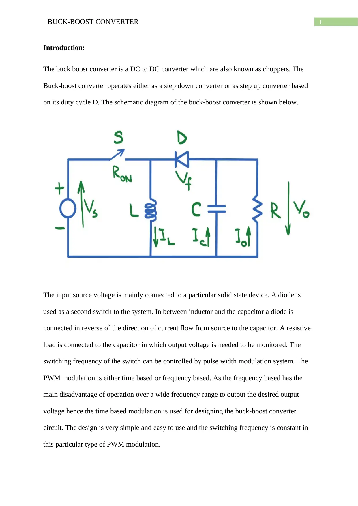
The buck boost converter is a DC to DC converter which are also known as choppers. The
Buck-boost converter operates either as a step down converter or as step up converter based
on its duty cycle D. The schematic diagram of the buck-boost converter is shown below.
The input source voltage is mainly connected to a particular solid state device. A diode is
used as a second switch to the system. In between inductor and the capacitor a diode is
connected in reverse of the direction of current flow from source to the capacitor. A resistive
load is connected to the capacitor in which output voltage is needed to be monitored. The
switching frequency of the switch can be controlled by pulse width modulation system. The
PWM modulation is either time based or frequency based. As the frequency based has the
main disadvantage of operation over a wide frequency range to output the desired output
voltage hence the time based modulation is used for designing the buck-boost converter
circuit. The design is very simple and easy to use and the switching frequency is constant in
this particular type of PWM modulation.
2BUCK-BOOST CONVERTER
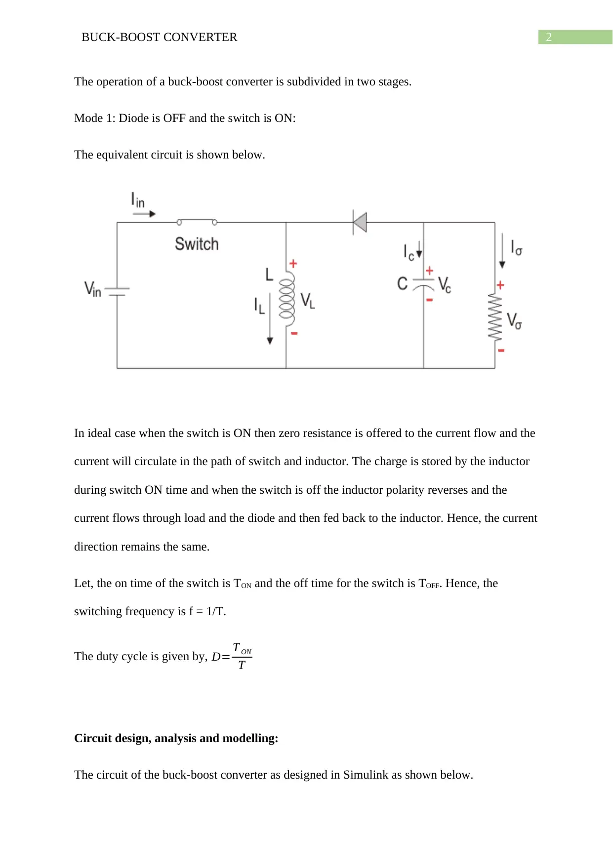
The operation of a buck-boost converter is subdivided in two stages.
Mode 1: Diode is OFF and the switch is ON:
The equivalent circuit is shown below.
In ideal case when the switch is ON then zero resistance is offered to the current flow and the
current will circulate in the path of switch and inductor. The charge is stored by the inductor
during switch ON time and when the switch is off the inductor polarity reverses and the
current flows through load and the diode and then fed back to the inductor. Hence, the current
direction remains the same.
Let, the on time of the switch is TON and the off time for the switch is TOFF. Hence, the
switching frequency is f = 1/T.
The duty cycle is given by, D= T ON
T
Circuit design, analysis and modelling:
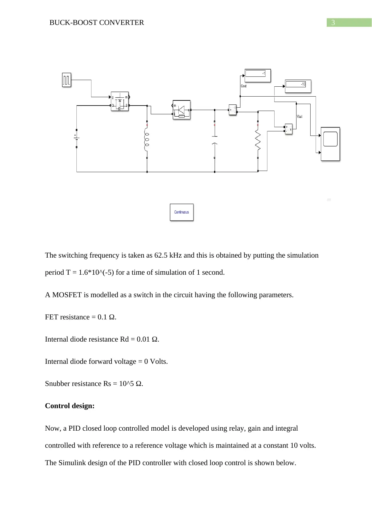
The circuit of the buck-boost converter as designed in Simulink as shown below.
⊘ This is a preview!⊘
Do you want full access?
Subscribe today to unlock all pages.

Trusted by 1+ million students worldwide
3BUCK-BOOST CONVERTER
The switching frequency is taken as 62.5 kHz and this is obtained by putting the simulation
period T = 1.6*10^(-5) for a time of simulation of 1 second.
A MOSFET is modelled as a switch in the circuit having the following parameters.
FET resistance = 0.1 Ω.
Internal diode resistance Rd = 0.01 Ω.
Internal diode forward voltage = 0 Volts.
Snubber resistance Rs = 10^5 Ω.
Control design:
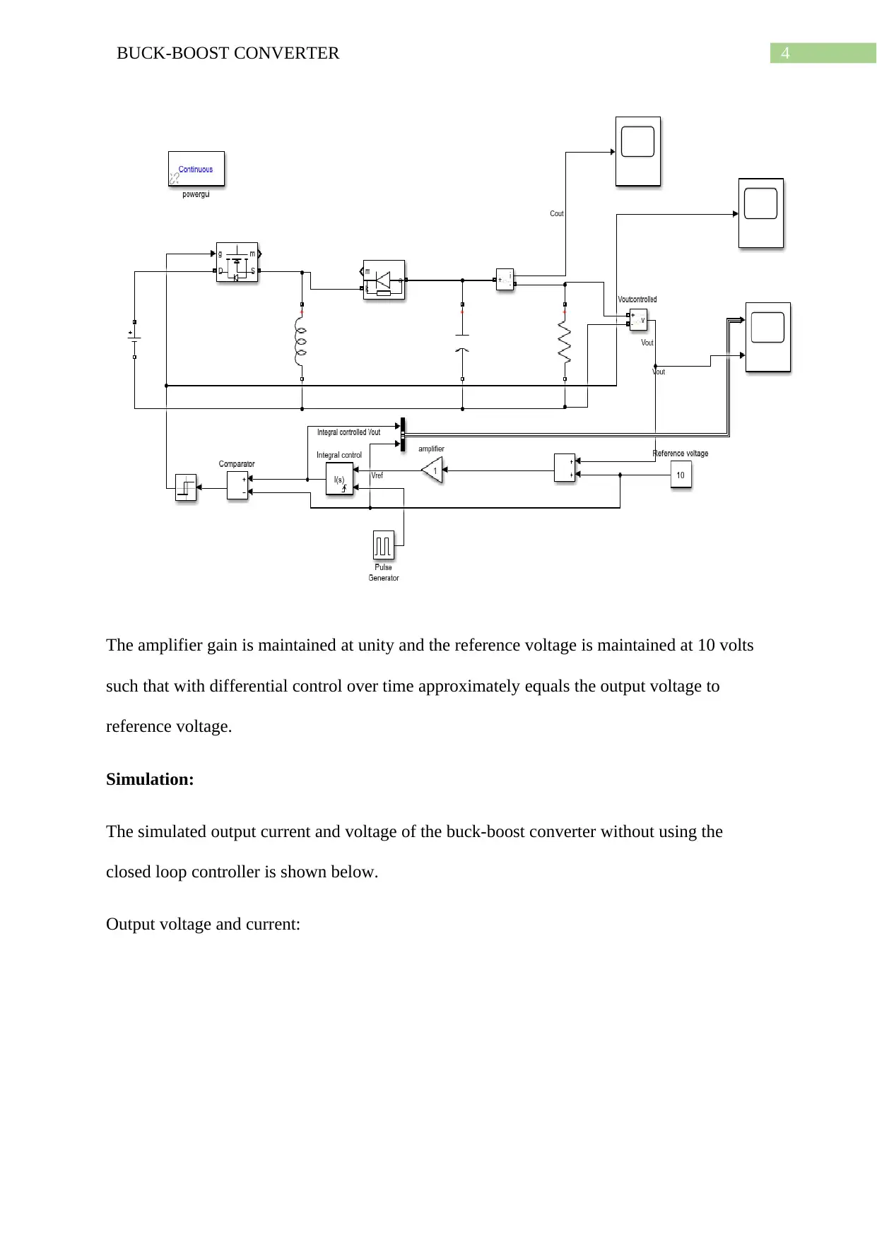
Now, a PID closed loop controlled model is developed using relay, gain and integral
controlled with reference to a reference voltage which is maintained at a constant 10 volts.
The Simulink design of the PID controller with closed loop control is shown below.
Paraphrase This Document
Need a fresh take? Get an instant paraphrase of this document with our AI Paraphraser
4BUCK-BOOST CONVERTER
The amplifier gain is maintained at unity and the reference voltage is maintained at 10 volts
such that with differential control over time approximately equals the output voltage to
reference voltage.
Simulation:
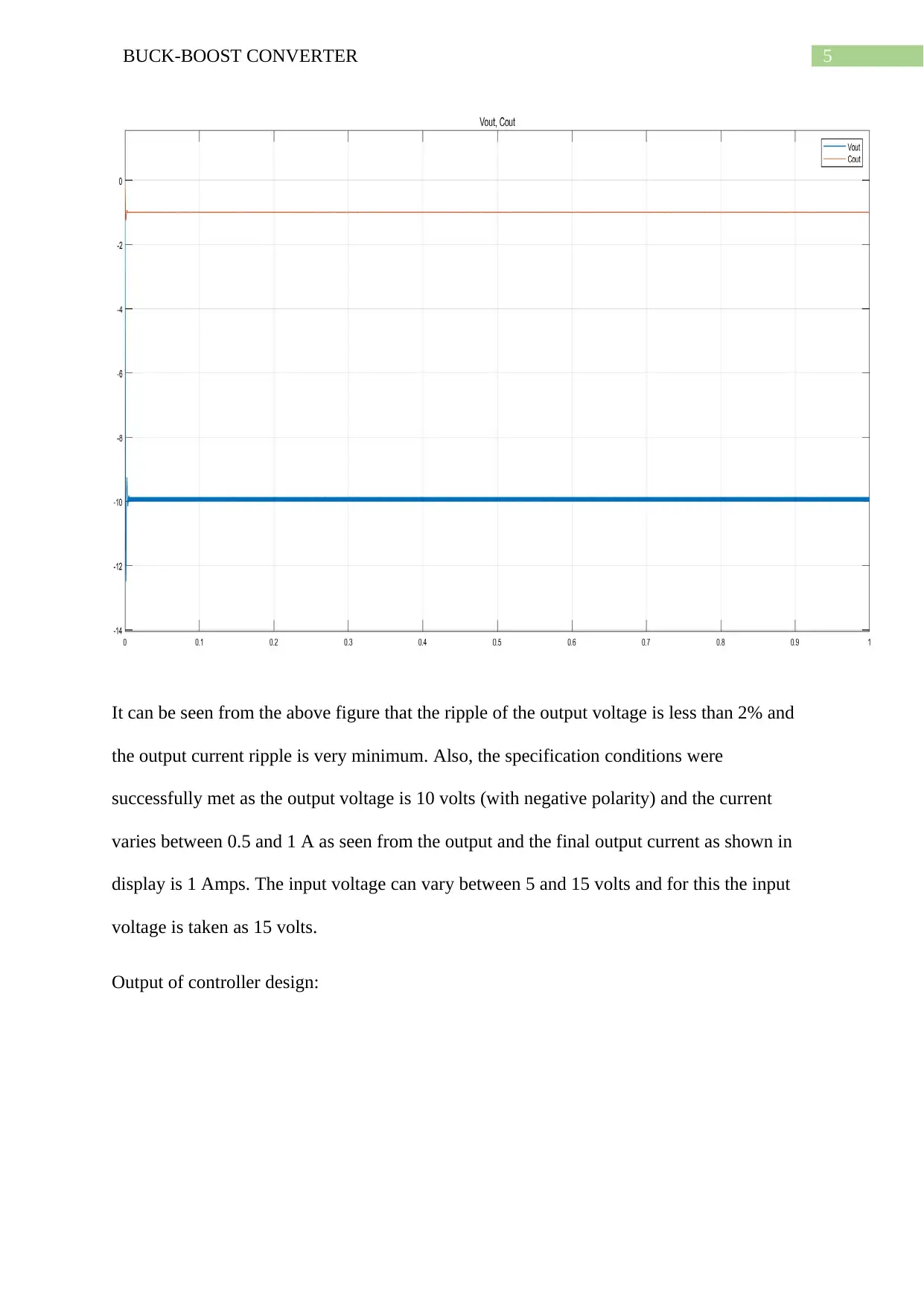
The simulated output current and voltage of the buck-boost converter without using the
closed loop controller is shown below.
Output voltage and current:
5BUCK-BOOST CONVERTER
It can be seen from the above figure that the ripple of the output voltage is less than 2% and
the output current ripple is very minimum. Also, the specification conditions were
successfully met as the output voltage is 10 volts (with negative polarity) and the current
varies between 0.5 and 1 A as seen from the output and the final output current as shown in
display is 1 Amps. The input voltage can vary between 5 and 15 volts and for this the input
voltage is taken as 15 volts.
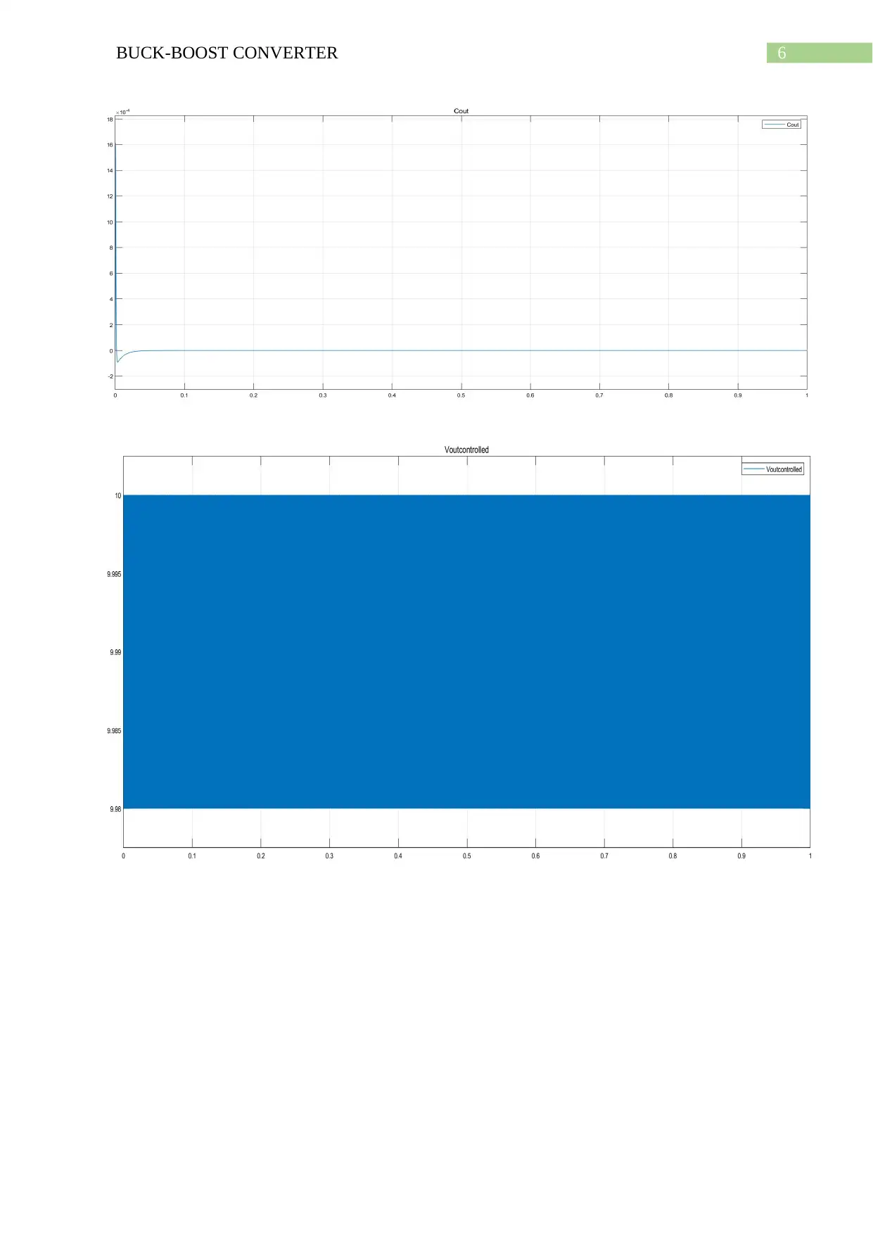
Output of controller design:
⊘ This is a preview!⊘
Do you want full access?
Subscribe today to unlock all pages.

Trusted by 1+ million students worldwide
6BUCK-BOOST CONVERTER
Paraphrase This Document
Need a fresh take? Get an instant paraphrase of this document with our AI Paraphraser
7BUCK-BOOST CONVERTER
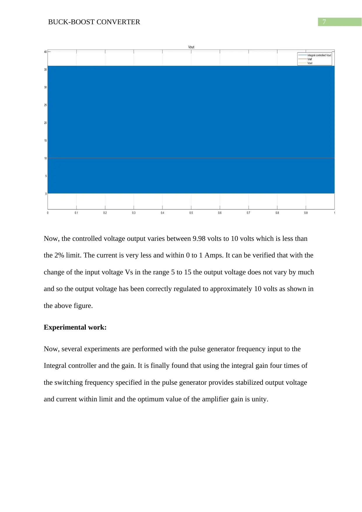
Now, the controlled voltage output varies between 9.98 volts to 10 volts which is less than
the 2% limit. The current is very less and within 0 to 1 Amps. It can be verified that with the
change of the input voltage Vs in the range 5 to 15 the output voltage does not vary by much
and so the output voltage has been correctly regulated to approximately 10 volts as shown in
the above figure.
Experimental work:
Now, several experiments are performed with the pulse generator frequency input to the
Integral controller and the gain. It is finally found that using the integral gain four times of
the switching frequency specified in the pulse generator provides stabilized output voltage
and current within limit and the optimum value of the amplifier gain is unity.

8BUCK-BOOST CONVERTER
Conclusion:
Hence, the design of Buck-boost converter design has been successfully implemented in
Simulink (a design based environment in MATLAB) and circuit design is simple and all the
design specifications were successfully met. Also, the design of the controller is obtained
with closed loop PID control strategy has been implemented appropriately as the controlled
output voltage and current are maintained within the specified range.
⊘ This is a preview!⊘
Do you want full access?
Subscribe today to unlock all pages.

Trusted by 1+ million students worldwide
1 out of 9
Related Documents
Your All-in-One AI-Powered Toolkit for Academic Success.
+13062052269
info@desklib.com
Available 24*7 on WhatsApp / Email
![[object Object]](/_next/static/media/star-bottom.7253800d.svg)
Unlock your academic potential
Copyright © 2020–2026 A2Z Services. All Rights Reserved. Developed and managed by ZUCOL.


