ProductsLogo
LogoStudy Documents
LogoAI Grader
LogoAI Answer
LogoAI Code Checker
LogoPlagiarism Checker
LogoAI Paraphraser
LogoAI Quiz
LogoAI Detector
PricingBlogAbout Us
logo

Computer System Components and Interactions

Verified

Added on  2020/09/03

|16
|4319
|281
AI Summary
This assignment delves into the components and interactions of computer systems. It covers the entry, reading, and fetching of data in the system, as well as the coordination between different components. The report discusses various aspects of computer architecture, including data signal processing, control units, arithmetic logic units, and other key features.

Contribute Materials

Your contribution can guide someone’s learning journey. Share your documents today.
Document Page
COMPUTER SYSTEM
ARCHITECTURE

Secure Best Marks with AI Grader

Need help grading? Try our AI Grader for instant feedback on your assignments.
Document Page
TABLE OF CONTENTS
INTRODUCTION...........................................................................................................................1
TASK 1 ...........................................................................................................................................1
P1 Method in which numeric and alphanumeric data can be coded within a computer system......1
P2 Way in which different types of data can be converted and stored in computer system.. 2
P3 Conversion of numeric data between different number system including floating point. 2
P4 Boolean logic operations...................................................................................................4
Truth table........................................................................................................................................7
TASK 2............................................................................................................................................7
P5 Key computer system components and their method of interaction.................................7
P6 Different types of memory that can be attached to a processor........................................9
P7 Role of polling and interrupts in allowing communication between processor and peripherals
..............................................................................................................................................10
TASK 3..........................................................................................................................................11
P8 Comparison between Reduced Instruction Set Computer (RISC) chips and Complex
Instruction Set Computer (CISC) chips................................................................................11
P9 Use of different processor registers in the fetch execute cycle.......................................11
CONCLUSION..............................................................................................................................12
REFERENCES..............................................................................................................................14
Document Page
INTRODUCTION
In the present era of digital advancements, it has become crucial to have an understanding of
the computer basics (Shironoshita, 2015) In the present undertaking the major components of the
system will be studied. In addition to this, ways in which data can be entered, stored and saved in
the computer systems will be discussed in the present piece of work. The report also covers the
understanding of the ways in which internal components of the system communicates. Also,
registers involved in the interaction are analysed.
TASK 1
P1 Method in which numeric and alphanumeric data can be coded within a computer system.
In order to represent numeric and alphanumeric data in a computer system, a sort of
coding is needed.
Coding of Numeric data in computer system:
Sign and magnitude: It is the representation of 1bit data, recognise that it is mostly the
leftmost data. In order to represent a sign, 0 is assigned for the positive integer whereas 1
is regarded as the sign for negative integer value (Shironoshita, 2015). For instance; -24
can be written as -11000 binary coding.
Two’s compliment: In this method, a positive integer is converted into a negative one by
making use of one’s and two’s compliments. For instance: 2's complement of -24 is
1111111111101000
Floating point: It is the way of representation of the approximation of a real number in
such a manner that it can support range and precision. For instance: 3.0 and 11.5.
Binary coded decimal: This method is utilised for the representation of the decimal
numbers with the help of binary codes 0 and 1 (Number Systems, Base Conversions and
Computer Data Representation, 2017).
Coding of Alphanumeric data in computer system:
Coding of character data: Coding of character is represented by the ASCII code. With the
help of this code, the numbers from 0-9 and alphabetical letter A-Z are encrypted in data
format. These are also known as the character strings.
1
Document Page
P2 Way in which different types of data can be converted and stored in computer system.
Data and information in the computer system are present in different forms. Some of them
includes text files, images or other multimedia forms such as audio and video files. Further, this
data can be converted and stored in many ways in the system. some of them are explained
further:
Text files: These files are just the sequence of numeric and alphanumeric characters.
There are certain codes settled for all these characters in the ASCII. For instance: code
for A is 65, for B it is 66 and so on. Thus, if the user wishes to convert a text file in a
binary code then a complete scanning from beginning to end is required.
Images: In this type of file conversion and storage, the field of view is divided into a fine
grid of sequence of little squares known as “pixels”. These pixels are filled with different
colours more or less uniform. At the time of image reading, these squares with the similar
colour are counted. These colour is then measured on the scale of 0 to 225.
Audio and Music: The sense of audio is based on the sensation of the variance in air
pressure. For this, microphone is used to convert the pressures into an analogue electric
signal. These signals ate further changed into a sequence of numbers by plotting the
curves on the graphs.
Video: The sound track of the file can be deal by the above-mentioned process. Now, for
the moving image part, the concept of synchronisation is used. For this, the video is
segregated into the different images with an added dimension of time.
Thus, these are the common formats of the files in which data can be stored and converted.
P3 Conversion of numeric data between different number system including floating point.
There are different ways in which numeric data can be converted into different machine
accepted format. Some of these data conversion tools are explained below along with the
relevant example:
Decimal: Octal to decimal- The radix of octal is 8 hence, any value from 0 to 7 can be written as
a single digit. For instance: An octal code is 123
Now, for converting it into a decimal system, the procedure is as follows:
(1*8^2) + (2*8^1) + (3*8^0) which results in 64+16+3=83 is the value of 1238 in decimal system
2

Paraphrase This Document

Need a fresh take? Get an instant paraphrase of this document with our AI Paraphraser
Document Page
Similarly, in case of binary and hexadecimal, their radix values that is 2 and 16,
respectively are used (Harris and Harris, 2015).
Octal: Decimal to octal- in this method of number conversion the digit is divided by the system
radix. Below is an example of converting into decimal to octal.
8 ˨86 Remainder:
8 ˨ 10 6
˨1 2
0 1
The answer is 126.
Similarly, rest number systems can also be converted as per their division to the radical
index of octal that is 8 (Decimal to binary converter, 2017)
Binary : In this, an example of decimal to binary will be represented. In this, the first step is to
write a decimal number and then make its division by 2 and it will give a result. The remainders
left will be in the form of binary, which means either 0 or 1. An example of this is as under :
15610
156/2 = 78; remainder = 0
78/2 = 39; remainder = 0
39/2 = 19; remainder = 1
19/2 = 9; remainder = 1
9/2 = 4; remainder = 1
4/2 = 2; remainder = 0
2/2 = 1; remainder = 0
2/1 = 2; remainder = 1
Seeing the remainders from below to top, we will get the result.
= 10011100
therefore,
15610 = 100111002
3
Document Page
P4 Boolean logic operations
In computer operations with the Boolean values, logic is used to describe the
electromagnetically charged memory locations.
Logic gates: It is a physical device that is used to execute the Boolean function given to
the systems. Thus, it performs the logical operations. There are different types of logic
gates that are used for different arithmetic operations to convert into logical. They also
change the numeric data into binary 0 and 1.
Truth tables: It is a mathematical table that is used for expressing the logical outcomes
performed by the Boolean logic gates (Monroe and et. al., 2014).
Use of logic gates in integrated circuits:
1. AND: It performs the multiplication operation given to the system (a*b). These gates are
symbolised as follows:
`Truth table for AND gate:
Input Output
A B
0 0 0
0 1 0
1 0 0
1 1 1
2. OR: These logic gates perform the addition function (a+b). These gates are symbolised as
follows:
Truth table for OR gate:
Input Output
A B
4
Document Page
0 0 0
0 1 1
1 0 1
1 1 1
3. NOT: These gates are known as inverters because of their action to reverse the input
value. These gates are symbolised as follows:
Truth table for NOT gate:
Input Output
A B
0 1
1 0
4. NAND: These gates perform the NOT of AND. That is reverse of (a*b). These gates are
symbolised as follows:
Truth table for NAND gate
Input Output
A B
0 0 1
0 1 1
1 0 1
1 1 0
5

Secure Best Marks with AI Grader

Need help grading? Try our AI Grader for instant feedback on your assignments.
Document Page
5. NOR: These gates perform the NOT of OR. That is reverse of (a+b). These gates are
symbolised as follows:
Truth table for NOR gate:
Input Output
A B
0 0 1
0 1 0
1 0 0
1 1 0
6. XNOR: These gate is a special functioned gated. It is used as half adder and full adder
subtracter. These gates are symbolised as follows:
Truth table for XOR gate:
Input Output
A B
0 0 1
0 1 0
1 0 0
1 1 1
Thus, these are the common logic gates that can be used for performing the logical
operations by the individual's functions based on the principle of gate.
An example of the connections of all these gates is being represented below :
6
Document Page
Truth table
A B C D Output X Output Y Output Z
0 0 0 0 0 0 0
0 1 0 0 0 1 0
0 0 1 0 0 1 0
0 1 1 0 0 1 0
1 0 0 1 0 1 0
1 1 0 1 1 1 0
1 0 1 1 1 1 0
1 1 1 1 1 1 1
This is the truth table of the following combination.
The following can be considered as an example of the combination of all the gates connected
together. As visible in the diagram above, D is a NOT gate, which means an inverter whereas B
is an OR gate and A is an AND gate. A combination of A and C are giving an XNOR gate as Z.
7
Document Page
The AND gate is considered as a basic digital logical gate which implies the conjunction
between the two whereas an OR gate implies logical disjunction. NOT gate is also called as an
inverter that has only one variable, either 1 or 0.
TASK 2
P5 Key computer system components and their method of interaction
Computer system, consists of various software and peripheral devices that are necessary
for it to function. The system has the following abilities:
Accept data and information
Input, store and implementation of instructions.
Perform arithmetical and logical operations
Output results as per the requirement of user.
There are different components of a computer system that plays major role in its
functioning, they are explained further:
Central Processing Unit: This component of a system is regarded as its brain that holds
the instructions of the program given by the user. There are further three major
components of a CPU which are Control Unit (CU), Arithmetic Logical Unit (ALU) and
Registers. The ALU and CU reads the data from either main or secondary memory. Later
with the help of cross-communication buses, this transmission of the data takes place.
Storage Unit: There exists two type of memory units in computer system, they are
primary and secondary memory. The primary memory of a system is in-built to it and
I/O systems: These units play a major role in the communication between the central
system and external environment (Amiri and Ali, 2013)..
8

Paraphrase This Document

Need a fresh take? Get an instant paraphrase of this document with our AI Paraphraser
Document Page
All these components are connected to each other by the computer buses. There are three
types of system buses: data, address and control. The data buses transfers data between the
computer peripherals connected to it. Address buses are used for the specified locations from
where data is taken. For instance: A system with 32bit address bus can address 2 raise to the
power 32 locations. A control is a bus that is used by the central system of the system to
communicate with the devices that are present within the computer. All the devices are
connected with each other through these different types of buses. Further, the internal
components of the computer system can interact with the peripheral attachments with these
communication lines.
P6 Different types of memory that can be attached to a processor.
Memory is regarded as an essential element of computer system. Without this feature the
system is barely of any use as it plays a significant role in saving and retrieving data. There are
basically two types of memory, namely primary and secondary.
Primary Memory: It is the volatile memory that is internal to the computer system. It comprises
of the RAM and ROM. This memory type renders the main working space to the system.
Primary memory can be further categorised in different form which are explained further:
RAM (Random Access Memory): It is regarded as the primary storage memory. It is due
to the fact that it is possible to randomly select and use any location for the saving and
retrieving of data. However, it should be noted that it is temp
9
Illustration 1: Interaction between different computer system components
Source: Vernon, 2007
Document Page
ROM (Read Only Memory): In this IC of the PC, data can be saved permanently. It
should be recognising that the program and data present in the ROM can only be read by
the central processing unit, that is it cannot be altered. The basic input and output
operations are stored in the ROM (Hasek and Markley, 2014).
PROM (Programmable Read Only Memory): It is another type of primary memory in
which the entered programs can be saved in the PROM chips. However, these
programmes cannot be modified or changed.
EPROM (Erasable Programmable Read Only Memory): This memory is widely used as it
overcomes the issues with the use of ROM and PROM. This memory chip can be
programmed by erasing the information stored earlier in it (Hasek and Markley, 2014).
Cache Memory: The speed of CPU is very high a compare to the access time of the main
memory. This can mismatch the operation timing and hence, a small memory chip is
attached between the processor unit and memory to eliminate this problem.
Registers: These are the special types of memory which are used to transfer data between
the different units of the computer. These are not the part of main memory but they can
store data and programs temporarily and pass it on as directed by the control unit of the
system.
Secondary Memory: This comprises of the permanent memory external to the system. It is
concerned with the magnetic memory and can be stored in various devices such as USBs,
magnetic tapes, floppy disks, etc. Some common type of secondary devices used are as follows:
Magnetic Tape: These are used for the large computers such as mainframe in which large
volume of the information is kept stored. These tapes can also be used in the PC in form
of cassettes.
Magnetic Disks: These disks are similar in the concept with the circular peripheral
devices used in gramophone. They rotate with a very high speed inside the computer
drive. In these disks data is stored on both the circular surfaces which is later read by the
system (Amiri and Ali, 2013).
Optical Disks: This is the recent type of secondary memory devices that have capacity to
store a large volume of data. It is further divided into three categories namely, compact
disks read only memory, write once read many and erasable optical disk.
10
Document Page
Thus, these are the different types of memories that are either in-built or connected to the
computer systems for performing different operations of saving, retrieving, etc.
P7 Role of polling and interrupts in allowing communication between processor and peripherals
Polling and interrupts plays a significant role in allowing communication between the
processor and peripherals. It should be recognising that a processor can perform only one
function at a time however, the functions are so fast to notice this fact. There exist various
peripheral which are connected to the system such as keyboard, mouse, USB drive, printers, hard
drive, etc. All these devices require attention from the central processing unit however, as stated
above there are various operations which are performed by the processor (Yu and et. al., 2015).
Thus, it needed a way in which it can identify the time when these peripherals need attention so
that it can stop the action and give them prior attention needed. There further exists two ways in
which processors and peripheral can communicate with each other, they are polling and
interrupts.
Polling is a method in which a program consistently checks for the status of a peripheral.
This action is performed to see of the devices are ready to send or receive the data. It
continuously polls the I/O devices to check if transmission can be made. On the other hand,
interrupts is a method of signalling to the CPU about the requirement of attention by a peripheral
device (Fenno and et. al., 2014). The devices are connected using interrupts line (a type of wire)
that signals the processors. In this way, polling and interrupts helps in making interaction
between the processor and attached peripherals.
These methods can be easily understood with an example mentioned below:
Picking up phone every few seconds to check if there is any call: Polling
Waiting for the phone to ring: Interrupts
TASK 3
P8 Comparison between Reduced Instruction Set Computer (RISC) chips and Complex
Instruction Set Computer (CISC) chips.
Reduced and complex instruction set computer chips are both the architectural designs of
CPU. The RISC designs use uniform instruction length for all instructions. Also, there are rigid
separate load/store instructions (Levy, 2014). RISC is prominent on the Software. There are low
11

Secure Best Marks with AI Grader

Need help grading? Try our AI Grader for instant feedback on your assignments.
Document Page
cycles per second in this processor deign. As different instructions are given in this computing
chips, more transistors are used for storing the memory. In addition to this, reduced instruction
set computer chips has a single clock. This too helps in getting more efficient code because of
the fact that a set of instruction is feed. The speed of the operation is higher in RISC as compared
to CISC as the execution time is lower in it.
On the other hand, complex instruction set computer chips is a processor design in which
single operation can implement several low-level operations. For instance: load from memory,
memory store, etc. These chips have calibre of multi-step addressing operations. This processor
design is simpler as there is no rigidity of executing different instructions for the operations. It
also sacrifices the number of cycles per instruction. CISC is prominent on Hardware having high
cycles per second. It has a multi-clock and load-store memory to memory is induced in the
instructions. In the CISC processor design it is easy to microcode new instructions. However, it
should be noted that CISC slows down the machine due to amount of clock time taken in
differentiating instructions (Siewiorek and Swarz, 2017).
P9 Use of different processor registers in the fetch execute cycle.
The fetch-execute cycle of a computer involves basically three steps:
1. Fetches the instructions of program from the memory of system.
2. States the requirements of the instruction.
3. Executing the actions required for decoding.
The cycle is consistently repeated by the CPU. In the accomplishment of each cycle, it
requires a certain set of circuits known as registers. There exists different type of registers that
are used in the fetch-execute cycle, they are as follows:
Program Counter (PC): This register is the part of internal storage which keeps the record
of memory address. In this the actions that are to be executed next are tracked for
continuing the operation (Harris and Harris, 2015).
Memory address register (MAR): The address present in the main memory which allows
user to read and write. It holds the address of a block of memory.
Memory data register (MDR) or Memory buffer register (MBR): It is a two-way register
that keeps the data which is fetched from the memory. This information is thus made
ready for the CPU to process.
12
Document Page
Current Instruction Register (CIR): It is a temporary platform at which the instruction
that are just fetched from the memory are kept. The addition information if required in
the cycle is added in this register with the help of address bus (Monroe and et. al., 2014).
Control unit (CU): This is regarded as the most crucial register of the cycle. A control
unit decodes the instructions present in the current instruction register. It selects the
needed resources such as data source register and specific arithmetic operation. Later by
coordinating the activation the decoding of the data takes place.
Arithmetic logic unit (ALU): This circuit of the processors system helps in performing
mathematical and logical operations.
CONCLUSION
In the present undertaking report, different aspects of the internal and external units of the
computer systems are studied. It has been analysed that in what way the data is entered, read and
fetched in the system. Further, interaction between the different components of the computer
architecture are discussed in the work piece.
13
Document Page
14
1 out of 16
[object Object]

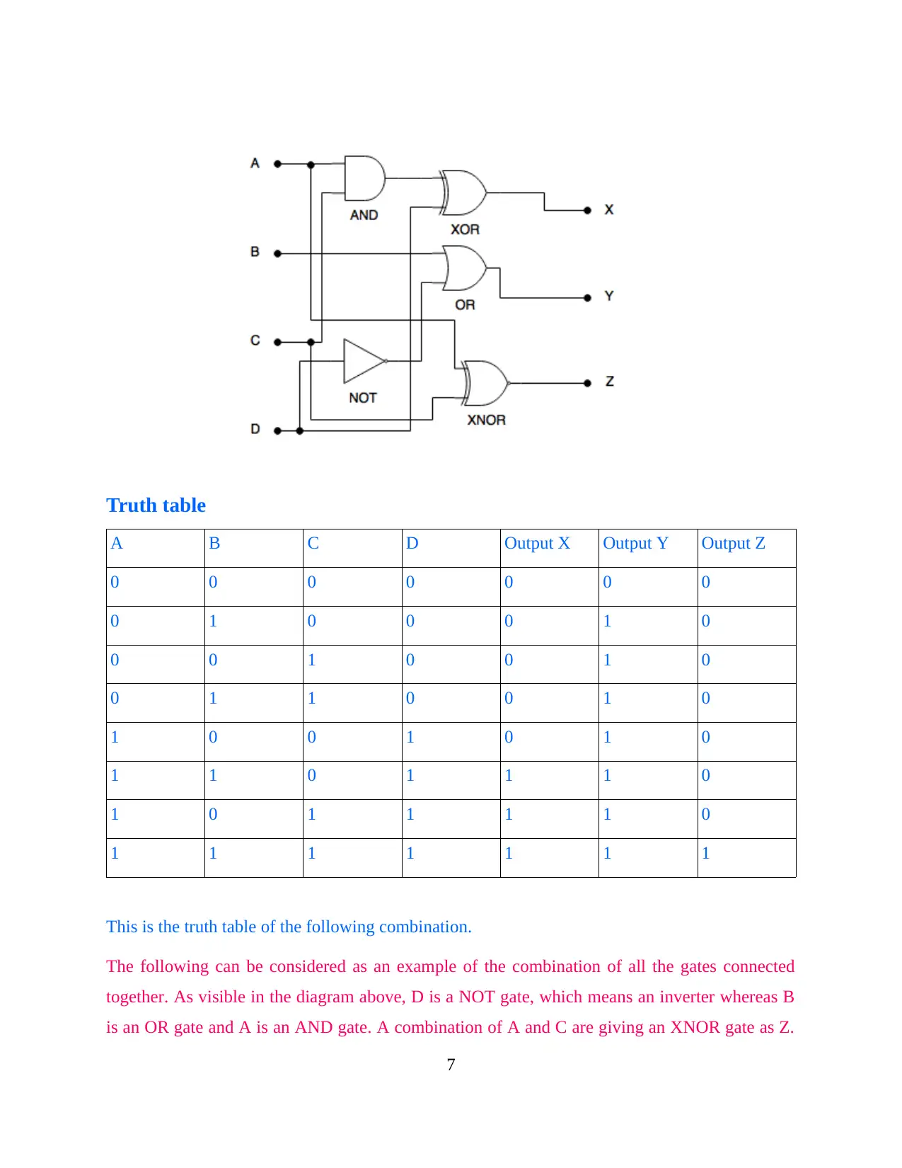
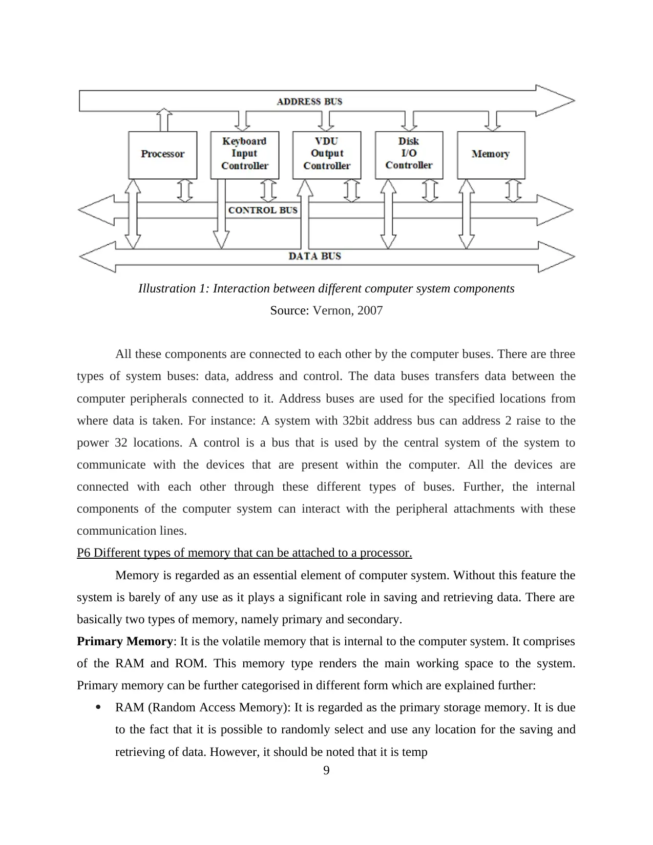
Your All-in-One AI-Powered Toolkit for Academic Success.

Available 24*7 on WhatsApp / Email

[object Object]