Power Amplifiers Design and Simulation | Report
VerifiedAdded on 2022/08/11
|27
|3863
|37
AI Summary
Contribute Materials
Your contribution can guide someone’s learning journey. Share your
documents today.
1
Student
Instructor
Title
POWER AMPLIFIERS DESIGN AND SIMULATION.
Date
Student
Instructor
Title
POWER AMPLIFIERS DESIGN AND SIMULATION.
Date
Secure Best Marks with AI Grader
Need help grading? Try our AI Grader for instant feedback on your assignments.
2
Table of Contents
1: INTRODUCTION.....................................................................................................................3
1.1: Finding Current Gain Ai.......................................................................................................5
1.2: Finding the Input Resistance.................................................................................................6
1.3: Finding Voltage Gain AV .....................................................................................................7
2: DESIGNING OF THE COMMON EMITTER POWER AMPLIFIER..............................9
2.1: Finding suitable collector load resistance of the circuit........................................................9
2.2: Finding the D.C operating point of the amplifier on the DC load line...............................10
2.3: Finding biasing resistor R1 and R2.....................................................................................15
2.4: Modification into Class B Amplifier..................................................................................18
2.5: Modification into Class AB Amplifier...............................................................................18
2.6: Modification into Class C Amplifier..................................................................................19
3: SIMULATION.........................................................................................................................21
4: RESULTS AND ANALYSIS..................................................................................................23
5: CONCLUSION........................................................................................................................25
6: REFERNCES...........................................................................................................................26
3
1: INTRODUCTION.
The project entails designing of class A amplifier using NPN transistor. The transistor naturally
operates as an amplifier in the active region where the collector current is linearly dependent on
the base current (ElProCus, 2020). Weak input signal at the base terminal of the transistor is
amplified when the base emitter junction of the transistor is forward biased. The polarity of the
input signal does not however, affects the biasing of the transistor (Tutorialspoint.com, 2018).
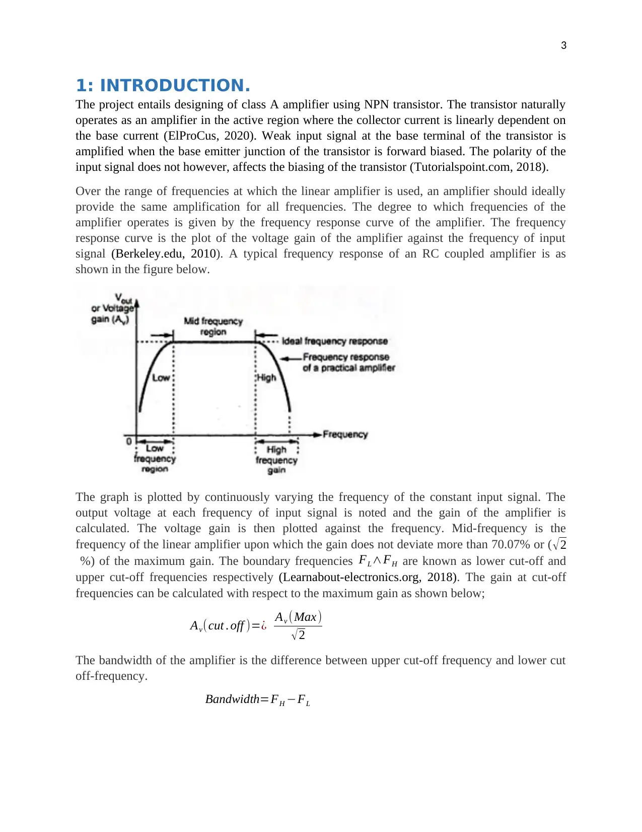
Over the range of frequencies at which the linear amplifier is used, an amplifier should ideally
provide the same amplification for all frequencies. The degree to which frequencies of the
amplifier operates is given by the frequency response curve of the amplifier. The frequency
response curve is the plot of the voltage gain of the amplifier against the frequency of input
signal (Berkeley.edu, 2010). A typical frequency response of an RC coupled amplifier is as
shown in the figure below.
The graph is plotted by continuously varying the frequency of the constant input signal. The
output voltage at each frequency of input signal is noted and the gain of the amplifier is
calculated. The voltage gain is then plotted against the frequency. Mid-frequency is the
frequency of the linear amplifier upon which the gain does not deviate more than 70.07% or ( √ 2
%) of the maximum gain. The boundary frequencies FL∧FH are known as lower cut-off and
upper cut-off frequencies respectively (Learnabout-electronics.org, 2018). The gain at cut-off
frequencies can be calculated with respect to the maximum gain as shown below;
Av(cut . off )=¿ Av (Max)
√2
The bandwidth of the amplifier is the difference between upper cut-off frequency and lower cut
off-frequency.
Bandwidth=FH −FL
1: INTRODUCTION.
The project entails designing of class A amplifier using NPN transistor. The transistor naturally
operates as an amplifier in the active region where the collector current is linearly dependent on
the base current (ElProCus, 2020). Weak input signal at the base terminal of the transistor is
amplified when the base emitter junction of the transistor is forward biased. The polarity of the
input signal does not however, affects the biasing of the transistor (Tutorialspoint.com, 2018).
Over the range of frequencies at which the linear amplifier is used, an amplifier should ideally
provide the same amplification for all frequencies. The degree to which frequencies of the
amplifier operates is given by the frequency response curve of the amplifier. The frequency
response curve is the plot of the voltage gain of the amplifier against the frequency of input
signal (Berkeley.edu, 2010). A typical frequency response of an RC coupled amplifier is as
shown in the figure below.
The graph is plotted by continuously varying the frequency of the constant input signal. The
output voltage at each frequency of input signal is noted and the gain of the amplifier is
calculated. The voltage gain is then plotted against the frequency. Mid-frequency is the
frequency of the linear amplifier upon which the gain does not deviate more than 70.07% or ( √ 2
%) of the maximum gain. The boundary frequencies FL∧FH are known as lower cut-off and
upper cut-off frequencies respectively (Learnabout-electronics.org, 2018). The gain at cut-off
frequencies can be calculated with respect to the maximum gain as shown below;
Av(cut . off )=¿ Av (Max)
√2
The bandwidth of the amplifier is the difference between upper cut-off frequency and lower cut
off-frequency.
Bandwidth=FH −FL
4
The amplifier amplifies properly within range of frequencies in the bandwidth. A good audio
amplifier must have bandwidth from 20 Hz to 20 kHz because that is the frequency range which
is audible.
The gain of the amplifier is the ratio of output power to input power. Gain can also be given by
the ratio of output voltage to input voltage as shown on the equation below.
Av=V out
V ¿
Or
Ap = Pout
P¿
Voltage gain of the amplifier can also be given in Decibels as shown in the expression below.
Voltage gain∈dB=20 log Av
Also, the power gain in Decibel is given by;
Power gain∈dB=10 log A p
When Av is greater than one, the dB gain is positive and when it is less than one, the dB gain is
negative. The negative and positive signs of dB indicate the amplification and attenuation
respectively.
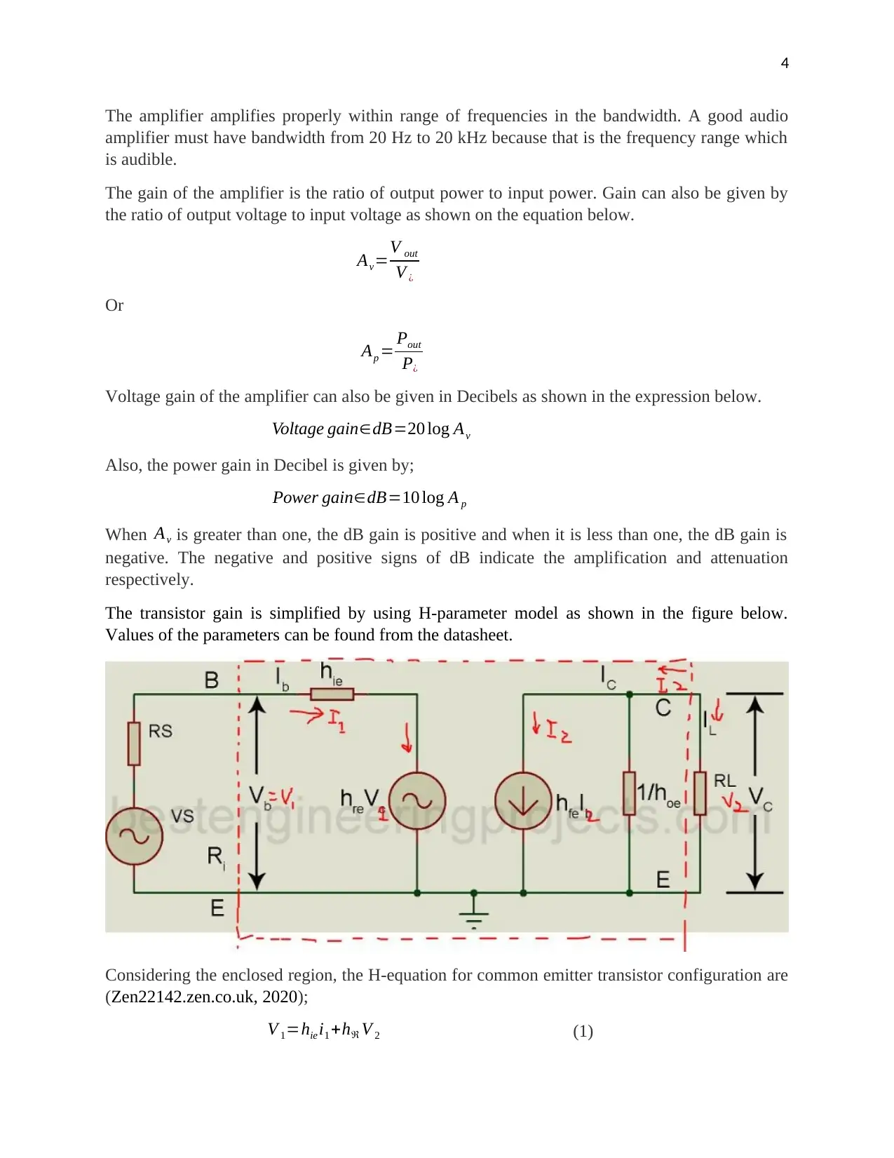
The transistor gain is simplified by using H-parameter model as shown in the figure below.
Values of the parameters can be found from the datasheet.
Considering the enclosed region, the H-equation for common emitter transistor configuration are
(Zen22142.zen.co.uk, 2020);
V 1=hie i1 +hℜ V 2 (1)
The amplifier amplifies properly within range of frequencies in the bandwidth. A good audio
amplifier must have bandwidth from 20 Hz to 20 kHz because that is the frequency range which
is audible.
The gain of the amplifier is the ratio of output power to input power. Gain can also be given by
the ratio of output voltage to input voltage as shown on the equation below.
Av=V out
V ¿
Or
Ap = Pout
P¿
Voltage gain of the amplifier can also be given in Decibels as shown in the expression below.
Voltage gain∈dB=20 log Av
Also, the power gain in Decibel is given by;
Power gain∈dB=10 log A p
When Av is greater than one, the dB gain is positive and when it is less than one, the dB gain is
negative. The negative and positive signs of dB indicate the amplification and attenuation
respectively.
The transistor gain is simplified by using H-parameter model as shown in the figure below.
Values of the parameters can be found from the datasheet.
Considering the enclosed region, the H-equation for common emitter transistor configuration are
(Zen22142.zen.co.uk, 2020);
V 1=hie i1 +hℜ V 2 (1)
Secure Best Marks with AI Grader
Need help grading? Try our AI Grader for instant feedback on your assignments.
5
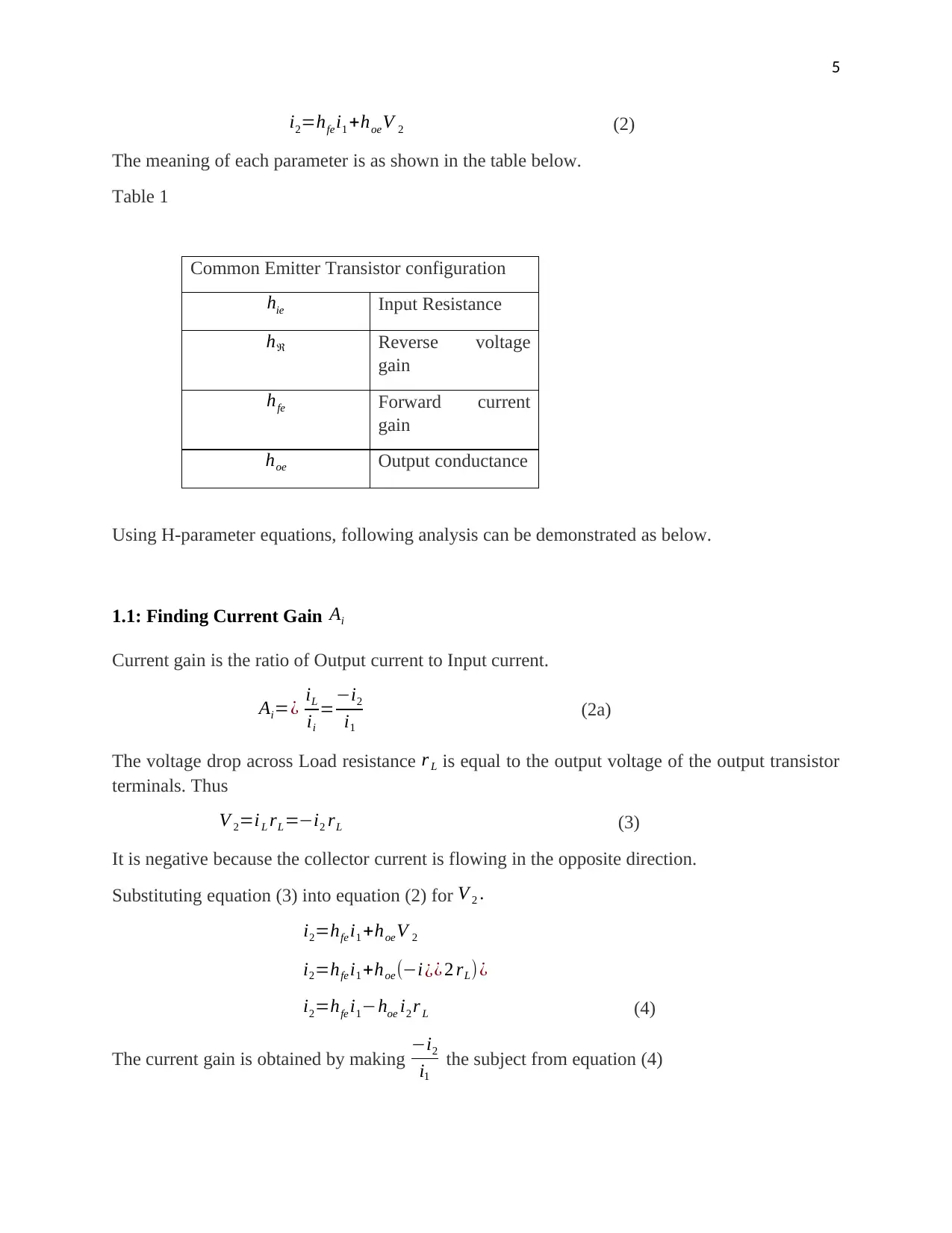
i2=hfei1 +hoeV 2 (2)
The meaning of each parameter is as shown in the table below.
Table 1
Common Emitter Transistor configuration
hie Input Resistance
hℜ Reverse voltage
gain
hfe Forward current
gain
hoe Output conductance
Using H-parameter equations, following analysis can be demonstrated as below.
1.1: Finding Current Gain Ai
Current gain is the ratio of Output current to Input current.
Ai=¿ iL
ii
=−i2
i1
(2a)
The voltage drop across Load resistance r L is equal to the output voltage of the output transistor
terminals. Thus
V 2=iL rL=−i2 rL (3)
It is negative because the collector current is flowing in the opposite direction.
Substituting equation (3) into equation (2) for V 2 .
i2=hfe i1 +hoe V 2
i2=hfe i1 +hoe (−i¿¿ 2 rL)¿
i2=hfe i1−hoe i2 r L (4)
The current gain is obtained by making −i2
i1
the subject from equation (4)
6
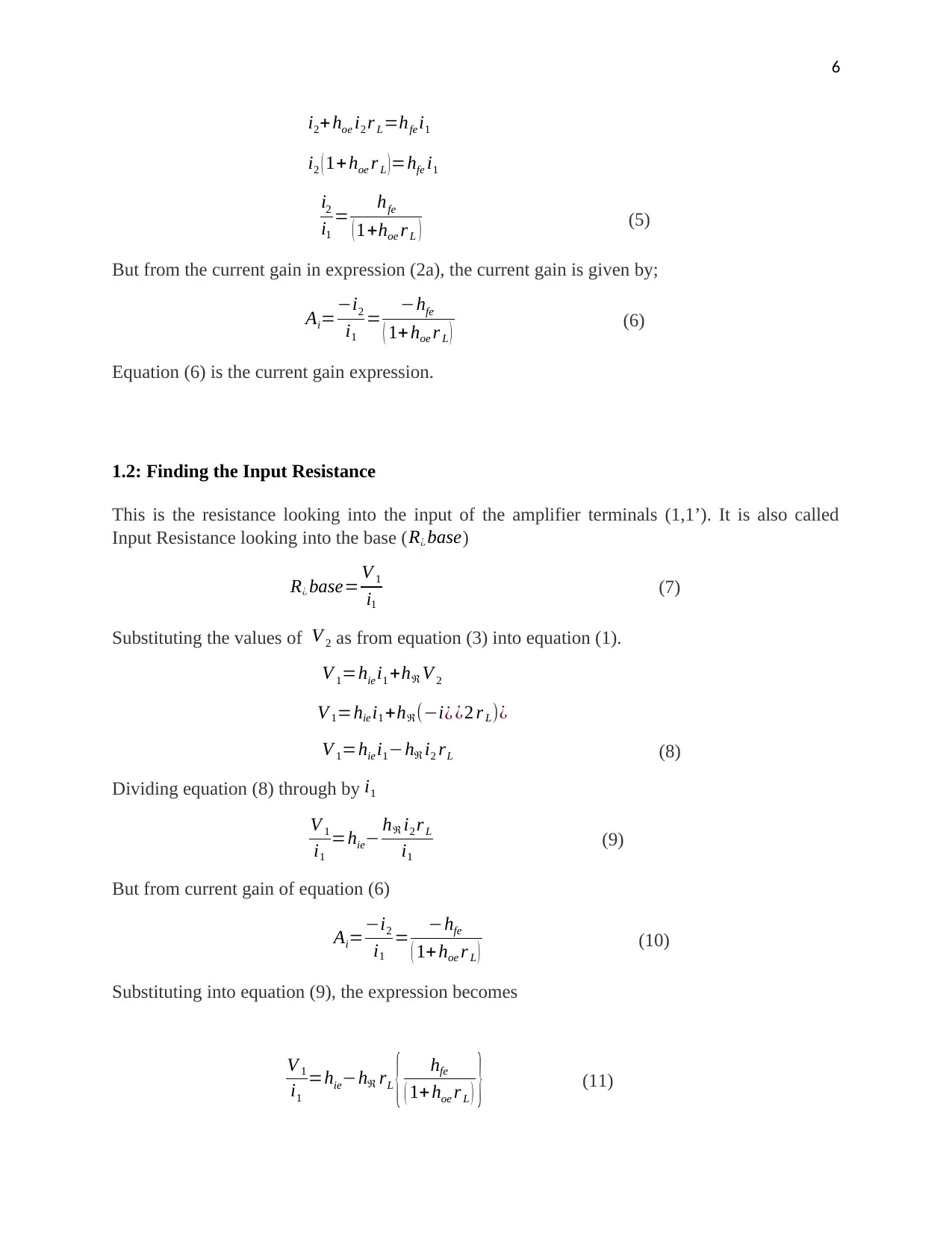
i2+ hoe i2 r L=hfe i1
i2 ( 1+hoe r L ) =hfe i1
i2
i1
= hfe
( 1+hoe r L ) (5)
But from the current gain in expression (2a), the current gain is given by;
Ai=−i2
i1
= −hfe
( 1+ hoe r L ) (6)
Equation (6) is the current gain expression.
1.2: Finding the Input Resistance
This is the resistance looking into the input of the amplifier terminals (1,1’). It is also called
Input Resistance looking into the base ( R¿ base)
R¿ base= V 1
i1
(7)
Substituting the values of V 2 as from equation (3) into equation (1).
V 1=hie i1 +hℜ V 2
V 1=hie i1 +hℜ(−i¿ ¿2 r L)¿
V 1=hie i1−hℜ i2 rL (8)
Dividing equation (8) through by i1
V 1
i1
=hie− hℜ i2 r L
i1
(9)
But from current gain of equation (6)
Ai=−i2
i1
= −hfe
( 1+ hoe r L ) (10)
Substituting into equation (9), the expression becomes
V 1
i1
=hie−hℜ rL { hfe
( 1+ hoe r L ) } (11)
7
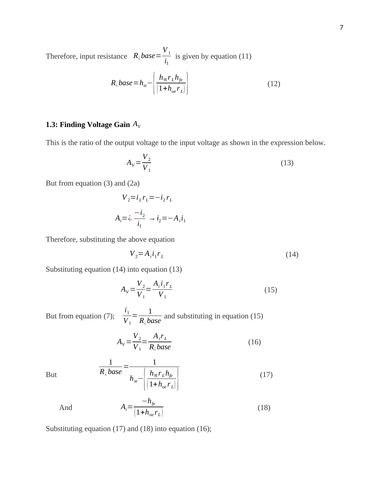
Therefore, input resistance R¿ base= V 1
i1
is given by equation (11)
R¿ base=hie− { hℜ r L hfe
( 1+hoe r L ) } (12)
1.3: Finding Voltage Gain AV
This is the ratio of the output voltage to the input voltage as shown in the expression below.
AV = V 2
V 1
(13)
But from equation (3) and (2a)
V 2=iL rL=−i2 rL
Ai=¿ −i2
i1
→ i2 =−Ai i1
Therefore, substituting the above equation
V 2= Ai i1 r L (14)
Substituting equation (14) into equation (13)
AV = V 2
V 1
= Ai i1 r L
V 1
(15)
But from equation (7); i1
V 1
= 1
R¿ base and substituting in equation (15)
AV = V 2
V 1
= Ai r L
R¿ base (16)
But
1
R¿ base = 1
hie− { hℜ r L hfe
( 1+ hoe r L ) } (17)
And Ai= −hfe
( 1+hoe rL ) (18)
Substituting equation (17) and (18) into equation (16);
Paraphrase This Document
Need a fresh take? Get an instant paraphrase of this document with our AI Paraphraser
8
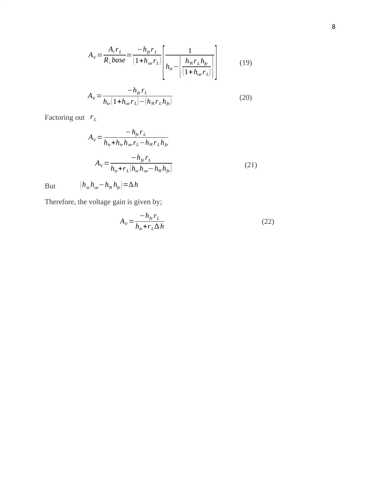
AV = Ai r L
R¿ base = −hfe r L
( 1+hoe rL )
[ 1
hie − { hℜ r L hfe
( 1+ hoe r L ) } ] (19)
AV = −hfe rL
hie ( 1+hoe r L ) − ( hℜ r L hfe ) (20)
Factoring out r L
AV = −hfe r L
hie +hie hoe rL−hℜ r L hfe
AV = −hfe rL
hie +r L ( hie hoe−hℜ hfe ) (21)
But ( hie hoe−hℜ hfe ) =∆ h
Therefore, the voltage gain is given by;
AV = −hfe rL
hie +r L ∆ h (22)
9
2: DESIGNING OF THE COMMON EMITTER POWER
AMPLIFIER.
The amplifier was designed by finding suitable parameters with regard to the desired operating
point. The design was done both in A.C and D.C analysis.
2.1: Finding suitable collector load resistance of the circuit.
The voltage gain and sinusoidal input voltage of the transistor power amplifier to be designed
has been specified in table 2 below.
Table 2
AV 5
v¿ 0.2 V p− p
Voltage gain the ratio of output voltage to the input sinusoidal voltage that is applied at the base
terminal of the transistor.
AV = vout
v¿
(23)
Using H-parameter, the voltage gain as in equation (22) was found to be;’
AV = −hfe rL
hie +r L ( hie hoe−hℜ hfe ) (24)
From the data sheet, H-parameters of the BC109 transistor is as shown in table (3) below
(Kitronik.co.uk, 2020)
Table 3
Common Emitter Transistor configuration
hie 5.5 kΩ
hℜ 3 ×10⁻⁴
hfe 370
hoe 30 μS
10
With parameters in table (3), the values in equation (25) can be substituted as demonstrated
below.
−5=¿ − ( 370 ) rL
( 5.5 kΩ ) +r L { ( 5.5 kΩ ×30 μS ) − ( 3 ×10−4 ×370 ) } (26)
Simplifying the equation;
5=¿ ( 370 ) r L
( 5500Ω ) + rL { ( 5.5 Ω× 30 S × 10−3 ) − ( 3 ×10−4 × 370 ) } (27)
5=¿ ( 370 ) r L
( 5500Ω )+rL {0.054 } (28)
Making load resistance the subject;
5 ( ( 5500 Ω ) +r L { 0.054 } )= ( 370 ) r L (29)
27500= ( 369.946 ) rL (30)
Therefore, the load resistance at the collector terminal is;
r L= 27500
369.946 =74.33 Ω (31)
This load resistance can also be denoted as;
r L=RC=74.33 Ω
2.2: Finding the D.C operating point of the amplifier on the DC load line.
In this project, voltage divider biasing was preferred. The trade-off of this type of biasing over
the other discussed methods is that there is reduced effects of temperature on current gain, β.
Current gain is very sensitive to the temperature and therefore, variation in temperature could
lead to inaccurate results and undesired conclusions. In addition, voltage divider biasing has its
collector quiescent current and common emitter quiescent voltage that are independent of the
value current gain provided biasing parameters are configured properly. In other words, in as
much as the value of current gain will be changing quiescent base current, the operating point of
the transistor amplifier however will be operating at a fixed point.
Secure Best Marks with AI Grader
Need help grading? Try our AI Grader for instant feedback on your assignments.
11
Analyzing the collector emitter loop of the transistor d.c circuit, the operating point of the class
A power amplifier can be established.
Applying the Kirchoff Voltage Law for this loop, the equation describing the relationship is as
shown by the expression below.
V CC −V RC −V CE=0 (32)
Where
V CC −¿This is the collector D.C voltage supplied to the collector terminal of the transistor.
V RC−¿This is the voltage drop across the resistor in series with the collector terminal.
V CE−¿This is the collector-emitter voltage of the transistor is DC analysis.
Rearranging equation (32) algebraically so as to form collector-emitter voltage the subject of the
formula results to the expression below.
V CE=V CC −V RC (33)
The DC voltage across the collector resistor can be defined by the DC collector current and the
resistance value of the collector resistor as illustrated in the equation below.
V RC=IC ( RC + RE ) (34)
Where;
I C−¿This is the DC collector current in the DC equivalent circuit.
RC –This is the collector resistance value.
RE−¿This is the emitter resistance value.
Substituting equation (32) into equation (33), the voltage across collector emitter can then be
expressed as;
12
V CE=V CC −IC ( RC + RE ) (35)
When the transistor is operating as power amplifier, then the desired region of operation should
be characterized by linear relationship between base current and collector current of the
transistor. Therefore, the transistor in a power amplifier configuration should operate in the
active region, which results to the desired amplification of the input base signals. In the active
region, the base current and collector current is related as in the expression below.
I C=β IB (36)
Where;
IB−¿This is DC base current in the DC equivalent circuit
β−¿This is the current gain of transistor.
By substituting equation (34) into equation (33), therefore, the collector-emitter voltage is
denoted as;
V CE=V CC −β IB ( RC + RE ) (37)
From equation (33) and (35), it can be concluded that as base current increases, collector current
increases accordingly. The overall effect leads to reduction of voltage across collector and
emitter. In this design, following parameters in table (4) were used.
Table 4;
V CC 12 V
β=hfe 370
RC 74.33 Ω
RE 0.5 kΩ
N/B β is the current gain retrieved from BC109 datasheet.
Substituting the values in equations (33) and (35)
V CE=12 V −I C ( RC + RE )
V CE=12V −β I B ( RC +RE ) } (38)
In the cut-off region, provided by the condition of insufficient biasing base voltage;
The base current is zero. Mathematically, the expressions are;
V B <V BE=0.7 V } Insufficient biasing (37)
13
Therefore, the transistor operates as an open circuit due to infinitely high resistance at the
depletion layer between collector emitter junction. As a results, no current is flowing through the
junction of the transistor.
I B=0 (39)
When base current is zero, then the collector current is also zero, hence equation (36) becomes;
V CE=V CC =12V ¿IC =0
When the transistor is operating in saturation region, then from equation (33);
V RC=V CC (40)
This implies that collector current is;
I C(sat)= V CC
( RC+RE ) (41)
Substituting the values from table 1, then the magnitude of DC collector current is computed as;
I C= 12 V
( 74.33+500 ) Ω =20.9 mA (42)
When this current is substituted in equation (36), then
V CE=0 (43)
When the transistor is operating in the active region, then the collector current should be limited
within the range of;
0<IC <20.9 mA (44)
And therefore, biasing base current should be also within the desired range so as to enable
transistor operate in the active region for linearity in the amplification of the signals. In
mathematical expression;
0<IB < 20.9
β mA (45)
Where;
β=180 for BC109 NPN transistor.
Substituting the value of current gain, the expression for biasing base current is;
0< I B < 0.056 mA (46)
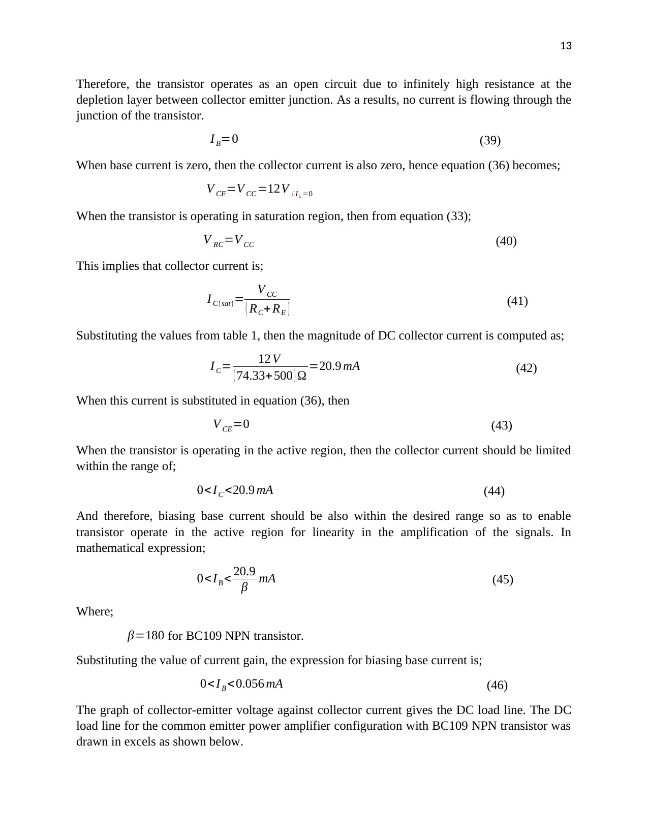
The graph of collector-emitter voltage against collector current gives the DC load line. The DC
load line for the common emitter power amplifier configuration with BC109 NPN transistor was
drawn in excels as shown below.
Therefore, the transistor operates as an open circuit due to infinitely high resistance at the
depletion layer between collector emitter junction. As a results, no current is flowing through the
junction of the transistor.
I B=0 (39)
When base current is zero, then the collector current is also zero, hence equation (36) becomes;
V CE=V CC =12V ¿IC =0
When the transistor is operating in saturation region, then from equation (33);
V RC=V CC (40)
This implies that collector current is;
I C(sat)= V CC
( RC+RE ) (41)
Substituting the values from table 1, then the magnitude of DC collector current is computed as;
I C= 12 V
( 74.33+500 ) Ω =20.9 mA (42)
When this current is substituted in equation (36), then
V CE=0 (43)
When the transistor is operating in the active region, then the collector current should be limited
within the range of;
0<IC <20.9 mA (44)
And therefore, biasing base current should be also within the desired range so as to enable
transistor operate in the active region for linearity in the amplification of the signals. In
mathematical expression;
0<IB < 20.9
β mA (45)
Where;
β=180 for BC109 NPN transistor.
Substituting the value of current gain, the expression for biasing base current is;
0< I B < 0.056 mA (46)
The graph of collector-emitter voltage against collector current gives the DC load line. The DC
load line for the common emitter power amplifier configuration with BC109 NPN transistor was
drawn in excels as shown below.
Paraphrase This Document
Need a fresh take? Get an instant paraphrase of this document with our AI Paraphraser
14
The input power of the class A amplifier is defined as the product of DC voltage supplied at the
collector and the DC collector current.
P¿=V CC IC (47)
For maximum power input, quiescent collector voltage, V CQ, and the quiescent collector current,
I CQ, are put into consideration. But from the DC load line, the quiescent collector current of the
power amplifier is a half the collector current at saturation. Substituting in equation (47), the
input power of the amplifier is given by;
P¿=V CC ICQ (48)
Where;
I CQ=1
2 IC (sat) (49)
I CQ=1
2 × 20.9 mA=10.45 mA
Using the collector current;
P¿=V CC
1
2 IC (sat) (50)
Where;
1
2 IC (sat)= V CC
2 Rc
(51)
15
Therefore, the maximum DC power input supplied to the power amplifier can be simplified as
the expression below.
P¿=V CC × V CC
2 Rc
(52)
P¿=V CC
2
2 Rc
(53)
Substituting the parameters in equation (48)
P¿=12V ×10.45 mA (54)
P¿=0.1254 W (55)
Proper biasing of the transistor is configured so that operating point lies at the center of the DC
load line. Therefore, the biasing base current is given by;
I BQ= I CQ
β (56)
Replacing the parameters as from the table and equation (49);
I BQ= 10.45 mA
370 (57)
I BQ=0.0282mA (58)
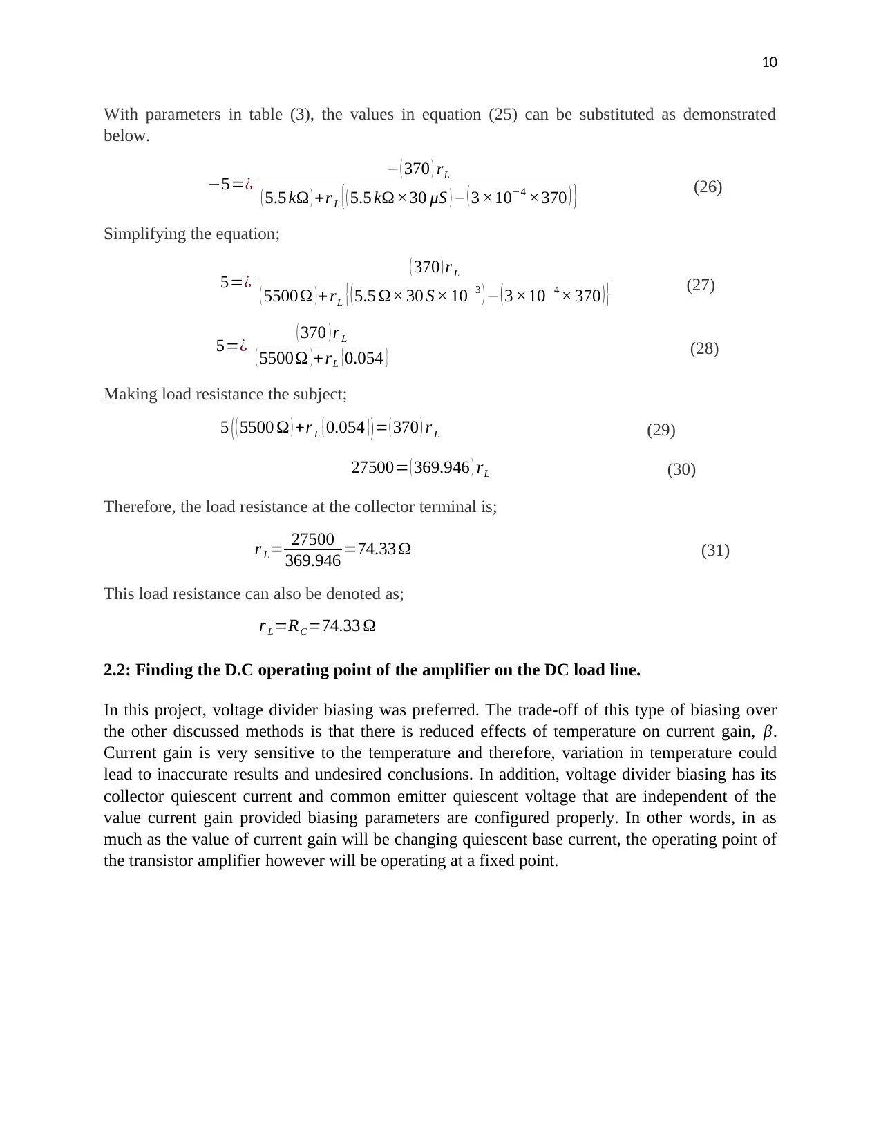
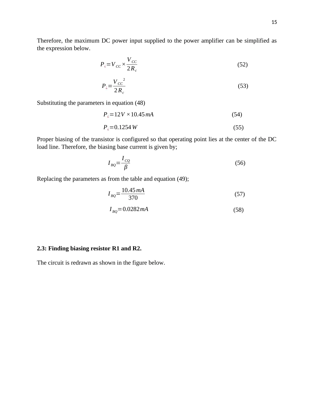
2.3: Finding biasing resistor R1 and R2.
The circuit is redrawn as shown in the figure below.
Therefore, the maximum DC power input supplied to the power amplifier can be simplified as
the expression below.
P¿=V CC × V CC
2 Rc
(52)
P¿=V CC
2
2 Rc
(53)
Substituting the parameters in equation (48)
P¿=12V ×10.45 mA (54)
P¿=0.1254 W (55)
Proper biasing of the transistor is configured so that operating point lies at the center of the DC
load line. Therefore, the biasing base current is given by;
I BQ= I CQ
β (56)
Replacing the parameters as from the table and equation (49);
I BQ= 10.45 mA
370 (57)
I BQ=0.0282mA (58)
2.3: Finding biasing resistor R1 and R2.
The circuit is redrawn as shown in the figure below.
16
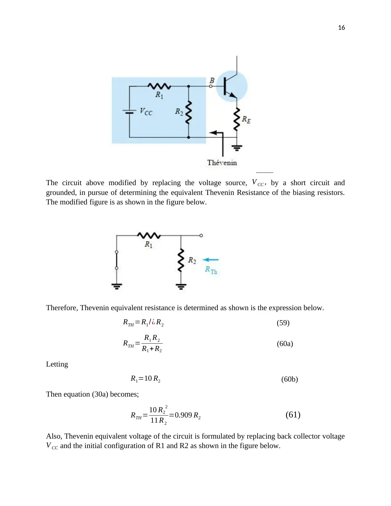
The circuit above modified by replacing the voltage source, V CC , by a short circuit and
grounded, in pursue of determining the equivalent Thevenin Resistance of the biasing resistors.
The modified figure is as shown in the figure below.
Therefore, Thevenin equivalent resistance is determined as shown is the expression below.
RTH =R1 /¿ R2 (59)
RTH = R1 R2
R1 + R2
(60a)
Letting
R1=10 R2 (60b)
Then equation (30a) becomes;
RTH =10 R2
2
11 R2
=0.909 R2 (61)
Also, Thevenin equivalent voltage of the circuit is formulated by replacing back collector voltage
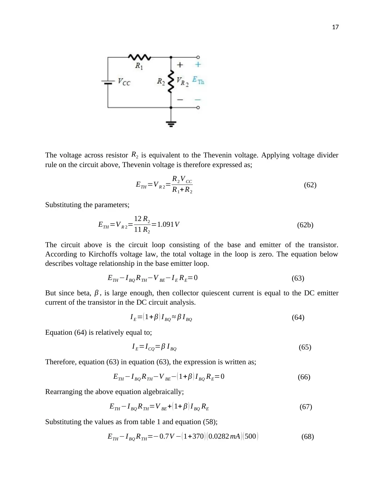
V CC and the initial configuration of R1 and R2 as shown in the figure below.
The circuit above modified by replacing the voltage source, V CC , by a short circuit and
grounded, in pursue of determining the equivalent Thevenin Resistance of the biasing resistors.
The modified figure is as shown in the figure below.
Therefore, Thevenin equivalent resistance is determined as shown is the expression below.
RTH =R1 /¿ R2 (59)
RTH = R1 R2
R1 + R2
(60a)
Letting
R1=10 R2 (60b)
Then equation (30a) becomes;
RTH =10 R2
2
11 R2
=0.909 R2 (61)
Also, Thevenin equivalent voltage of the circuit is formulated by replacing back collector voltage
V CC and the initial configuration of R1 and R2 as shown in the figure below.
Secure Best Marks with AI Grader
Need help grading? Try our AI Grader for instant feedback on your assignments.
17
The voltage across resistor R2 is equivalent to the Thevenin voltage. Applying voltage divider
rule on the circuit above, Thevenin voltage is therefore expressed as;
ETH =V R 2= R2 V CC
R1+R2
(62)
Substituting the parameters;
ETH =V R 2=12 R2
11 R2
=1.091V (62b)
The circuit above is the circuit loop consisting of the base and emitter of the transistor.
According to Kirchoffs voltage law, the total voltage in the loop is zero. The equation below
describes voltage relationship in the base emitter loop.
ETH −IBQ RTH−V BE−IE RE=0 (63)
But since beta, β , is large enough, then collector quiescent current is equal to the DC emitter
current of the transistor in the DC circuit analysis.
IE = ( 1+β ) IBQ ≈ β I BQ (64)
Equation (64) is relatively equal to;
I E =ICQ=β I BQ (65)
Therefore, equation (63) in equation (63), the expression is written as;
ETH −I BQ RTH−V BE− ( 1+β ) I BQ RE=0 (66)
Rearranging the above equation algebraically;
ETH −I BQ RTH=V BE + ( 1+ β ) I BQ RE (67)
Substituting the values as from table 1 and equation (58);
ETH −I BQ RTH=−0.7V − ( 1+370 ) ( 0.0282 mA ) ( 500 ) (68)
18
ETH −I BQ RTH=−5.931 V (69)
From equation (61) and (62), Thevenin equivalent parameters envisaged into them are
substituted in equation (69) leading to the overall expression below.
[ 1.091V ] − ( 0.0282mA ) [ 0.909 R2 ]=−5.931V (70)
Simplifying equation (40),
0.000256 R2=7.022 (72)
From equation 72, the value of resistor R2 was found to be;
R2= 7.022
0.000256 =27.4 kΩ (73)
Therefore, in the design, the value of resistor R2 is equal to 27.4 kΩ and R1 is approximately
274 kΩ
The D.C biasing circuit has the following parameters as shown in table 5.
Table 5
R1 270 kΩ
R2 27 kΩ
V CC 12 V
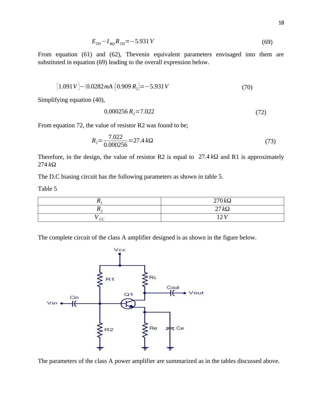
The complete circuit of the class A amplifier designed is as shown in the figure below.
The parameters of the class A power amplifier are summarized as in the tables discussed above.
ETH −I BQ RTH=−5.931 V (69)
From equation (61) and (62), Thevenin equivalent parameters envisaged into them are
substituted in equation (69) leading to the overall expression below.
[ 1.091V ] − ( 0.0282mA ) [ 0.909 R2 ]=−5.931V (70)
Simplifying equation (40),
0.000256 R2=7.022 (72)
From equation 72, the value of resistor R2 was found to be;
R2= 7.022
0.000256 =27.4 kΩ (73)
Therefore, in the design, the value of resistor R2 is equal to 27.4 kΩ and R1 is approximately
274 kΩ
The D.C biasing circuit has the following parameters as shown in table 5.
Table 5
R1 270 kΩ
R2 27 kΩ
V CC 12 V
The complete circuit of the class A amplifier designed is as shown in the figure below.
The parameters of the class A power amplifier are summarized as in the tables discussed above.
19
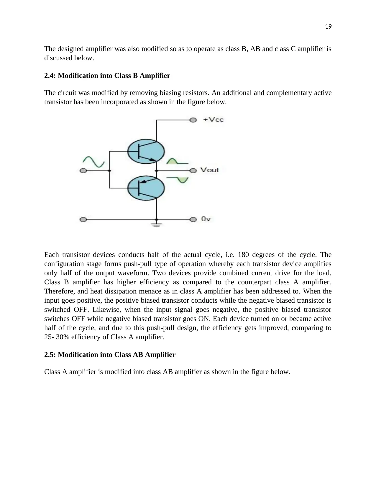
The designed amplifier was also modified so as to operate as class B, AB and class C amplifier is
discussed below.
2.4: Modification into Class B Amplifier
The circuit was modified by removing biasing resistors. An additional and complementary active
transistor has been incorporated as shown in the figure below.
Each transistor devices conducts half of the actual cycle, i.e. 180 degrees of the cycle. The
configuration stage forms push-pull type of operation whereby each transistor device amplifies
only half of the output waveform. Two devices provide combined current drive for the load.
Class B amplifier has higher efficiency as compared to the counterpart class A amplifier.
Therefore, and heat dissipation menace as in class A amplifier has been addressed to. When the
input goes positive, the positive biased transistor conducts while the negative biased transistor is
switched OFF. Likewise, when the input signal goes negative, the positive biased transistor
switches OFF while negative biased transistor goes ON. Each device turned on or became active
half of the cycle, and due to this push-pull design, the efficiency gets improved, comparing to
25- 30% efficiency of Class A amplifier.
2.5: Modification into Class AB Amplifier
Class A amplifier is modified into class AB amplifier as shown in the figure below.
Paraphrase This Document
Need a fresh take? Get an instant paraphrase of this document with our AI Paraphraser
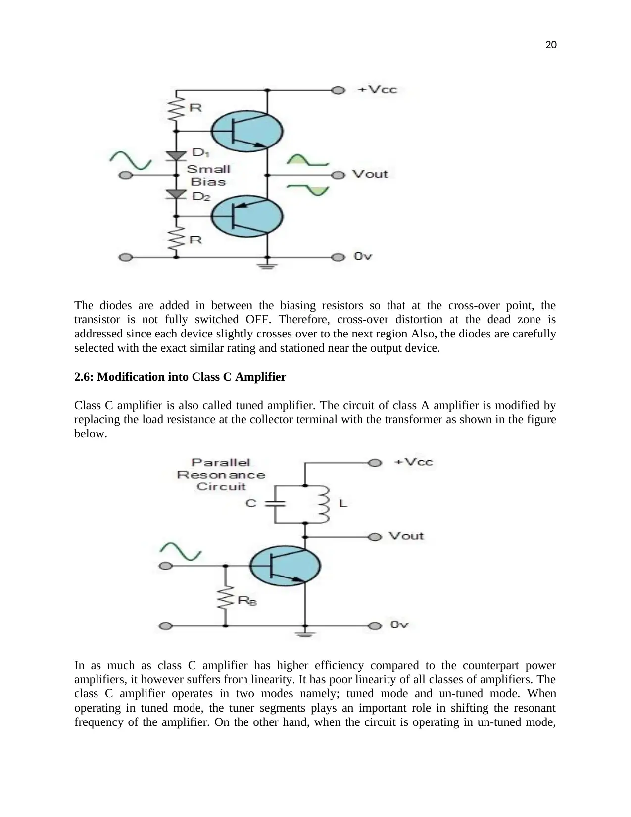
20
The diodes are added in between the biasing resistors so that at the cross-over point, the
transistor is not fully switched OFF. Therefore, cross-over distortion at the dead zone is
addressed since each device slightly crosses over to the next region Also, the diodes are carefully
selected with the exact similar rating and stationed near the output device.
2.6: Modification into Class C Amplifier
Class C amplifier is also called tuned amplifier. The circuit of class A amplifier is modified by
replacing the load resistance at the collector terminal with the transformer as shown in the figure
below.
In as much as class C amplifier has higher efficiency compared to the counterpart power
amplifiers, it however suffers from linearity. It has poor linearity of all classes of amplifiers. The
class C amplifier operates in two modes namely; tuned mode and un-tuned mode. When
operating in tuned mode, the tuner segments plays an important role in shifting the resonant
frequency of the amplifier. On the other hand, when the circuit is operating in un-tuned mode,
21
the tuner segment is isolated from the circuit. Resonant frequency depends on the value of the
inductor and capacitor as in the equation below.
f r= 1
2 π √ LC (74)
Where;
f r−¿Is the resonant frequency
L∧C−¿Are the inductor and capacitor value of the active component.
the tuner segment is isolated from the circuit. Resonant frequency depends on the value of the
inductor and capacitor as in the equation below.
f r= 1
2 π √ LC (74)
Where;
f r−¿Is the resonant frequency
L∧C−¿Are the inductor and capacitor value of the active component.
22
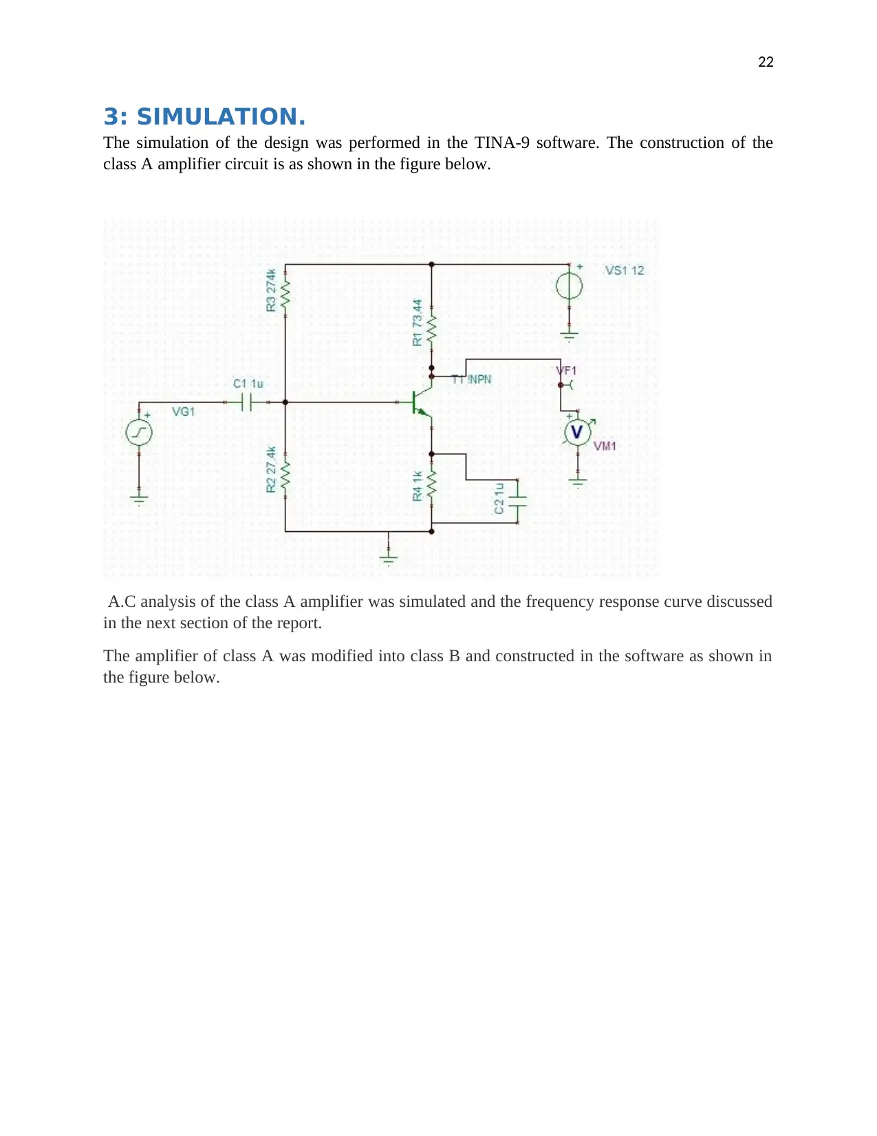
3: SIMULATION.
The simulation of the design was performed in the TINA-9 software. The construction of the
class A amplifier circuit is as shown in the figure below.
A.C analysis of the class A amplifier was simulated and the frequency response curve discussed
in the next section of the report.
The amplifier of class A was modified into class B and constructed in the software as shown in
the figure below.
Secure Best Marks with AI Grader
Need help grading? Try our AI Grader for instant feedback on your assignments.
23
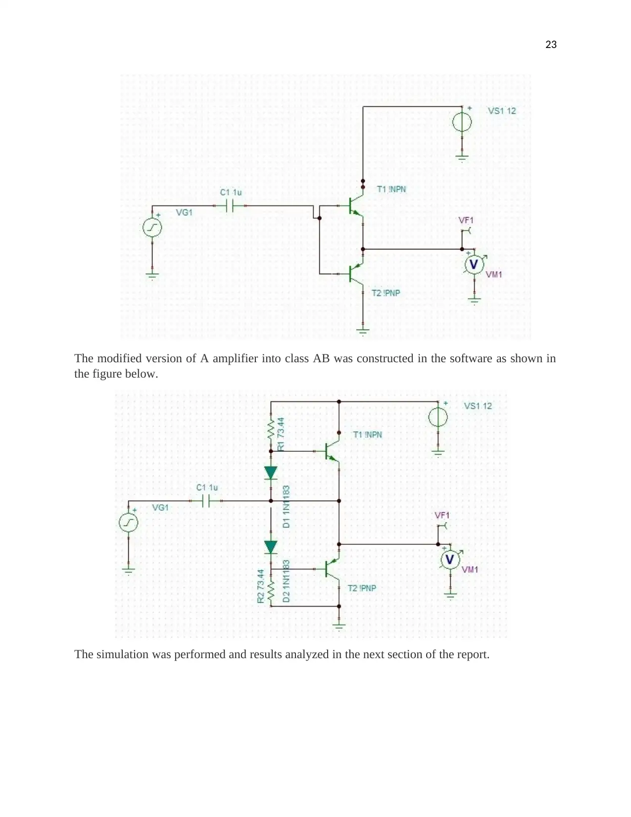
The modified version of A amplifier into class AB was constructed in the software as shown in
the figure below.
The simulation was performed and results analyzed in the next section of the report.
The modified version of A amplifier into class AB was constructed in the software as shown in
the figure below.
The simulation was performed and results analyzed in the next section of the report.
24
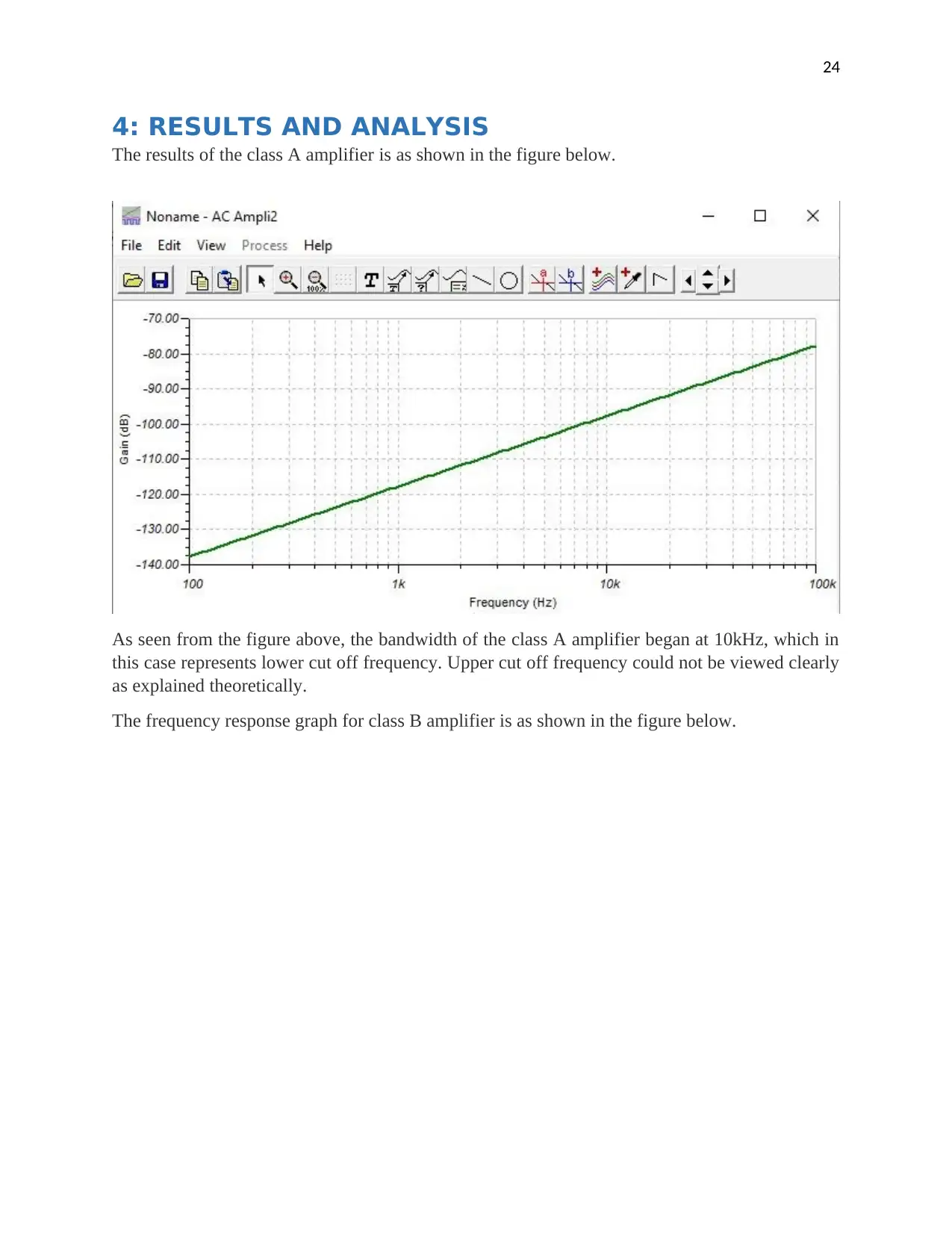
4: RESULTS AND ANALYSIS
The results of the class A amplifier is as shown in the figure below.
As seen from the figure above, the bandwidth of the class A amplifier began at 10kHz, which in
this case represents lower cut off frequency. Upper cut off frequency could not be viewed clearly
as explained theoretically.
The frequency response graph for class B amplifier is as shown in the figure below.
25
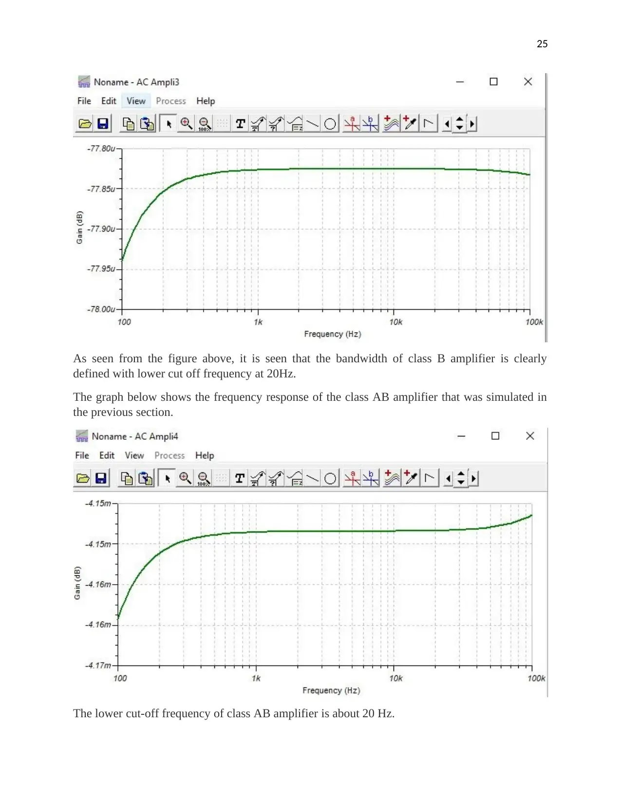
As seen from the figure above, it is seen that the bandwidth of class B amplifier is clearly
defined with lower cut off frequency at 20Hz.
The graph below shows the frequency response of the class AB amplifier that was simulated in
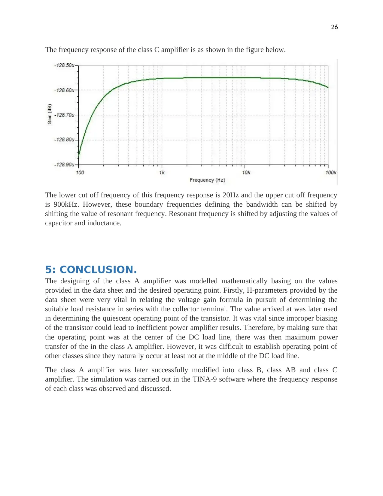
the previous section.
The lower cut-off frequency of class AB amplifier is about 20 Hz.
As seen from the figure above, it is seen that the bandwidth of class B amplifier is clearly
defined with lower cut off frequency at 20Hz.
The graph below shows the frequency response of the class AB amplifier that was simulated in
the previous section.
The lower cut-off frequency of class AB amplifier is about 20 Hz.
Paraphrase This Document
Need a fresh take? Get an instant paraphrase of this document with our AI Paraphraser
26
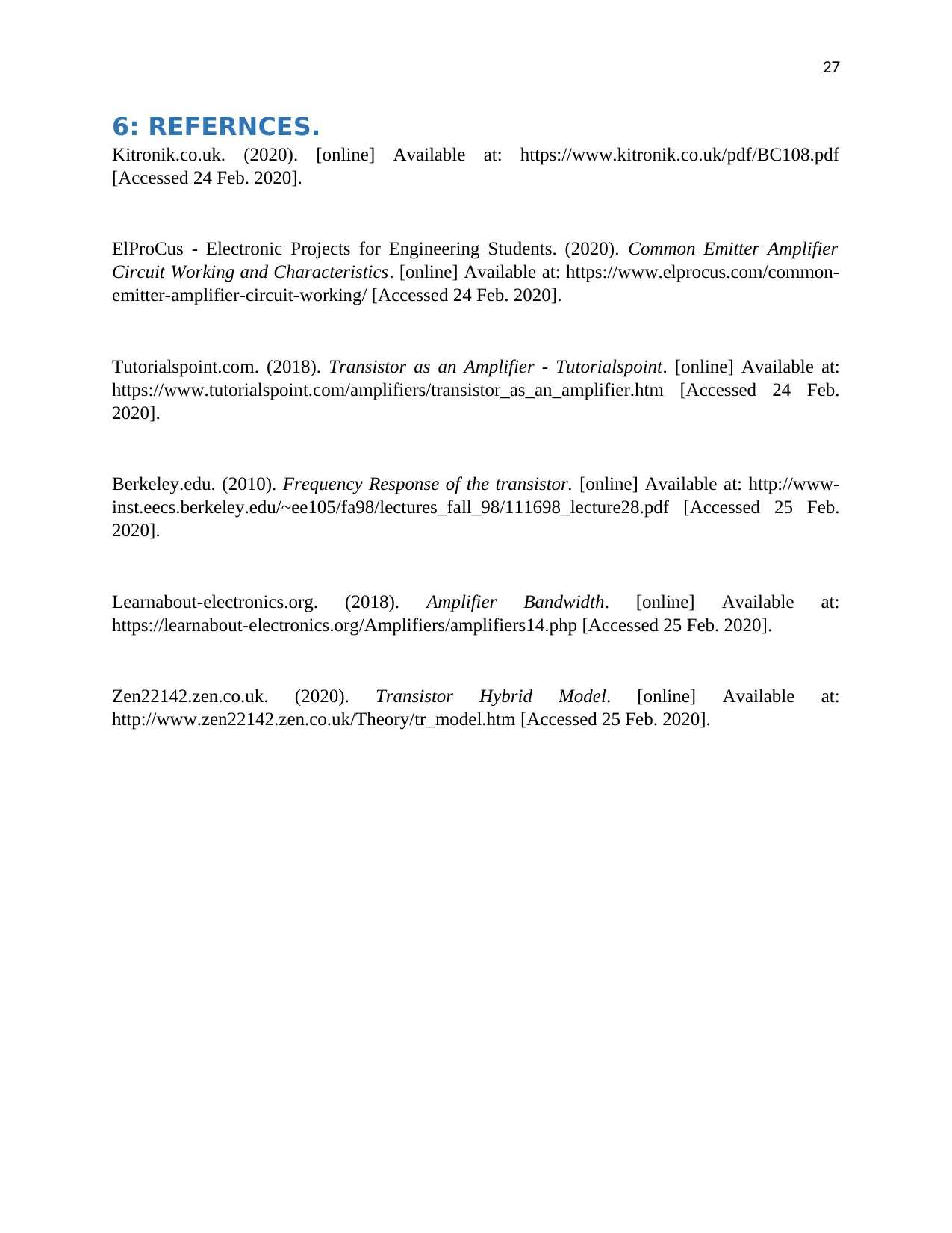
The frequency response of the class C amplifier is as shown in the figure below.
The lower cut off frequency of this frequency response is 20Hz and the upper cut off frequency
is 900kHz. However, these boundary frequencies defining the bandwidth can be shifted by
shifting the value of resonant frequency. Resonant frequency is shifted by adjusting the values of
capacitor and inductance.
5: CONCLUSION.
The designing of the class A amplifier was modelled mathematically basing on the values
provided in the data sheet and the desired operating point. Firstly, H-parameters provided by the
data sheet were very vital in relating the voltage gain formula in pursuit of determining the
suitable load resistance in series with the collector terminal. The value arrived at was later used
in determining the quiescent operating point of the transistor. It was vital since improper biasing
of the transistor could lead to inefficient power amplifier results. Therefore, by making sure that
the operating point was at the center of the DC load line, there was then maximum power
transfer of the in the class A amplifier. However, it was difficult to establish operating point of
other classes since they naturally occur at least not at the middle of the DC load line.
The class A amplifier was later successfully modified into class B, class AB and class C
amplifier. The simulation was carried out in the TINA-9 software where the frequency response
of each class was observed and discussed.
27
6: REFERNCES.
Kitronik.co.uk. (2020). [online] Available at: https://www.kitronik.co.uk/pdf/BC108.pdf
[Accessed 24 Feb. 2020].
ElProCus - Electronic Projects for Engineering Students. (2020). Common Emitter Amplifier
Circuit Working and Characteristics. [online] Available at: https://www.elprocus.com/common-
emitter-amplifier-circuit-working/ [Accessed 24 Feb. 2020].
Tutorialspoint.com. (2018). Transistor as an Amplifier - Tutorialspoint. [online] Available at:
https://www.tutorialspoint.com/amplifiers/transistor_as_an_amplifier.htm [Accessed 24 Feb.
2020].
Berkeley.edu. (2010). Frequency Response of the transistor. [online] Available at: http://www-
inst.eecs.berkeley.edu/~ee105/fa98/lectures_fall_98/111698_lecture28.pdf [Accessed 25 Feb.
2020].
Learnabout-electronics.org. (2018). Amplifier Bandwidth. [online] Available at:
https://learnabout-electronics.org/Amplifiers/amplifiers14.php [Accessed 25 Feb. 2020].
Zen22142.zen.co.uk. (2020). Transistor Hybrid Model. [online] Available at:
http://www.zen22142.zen.co.uk/Theory/tr_model.htm [Accessed 25 Feb. 2020].
1 out of 27
Related Documents


Your All-in-One AI-Powered Toolkit for Academic Success.
+13062052269
info@desklib.com
Available 24*7 on WhatsApp / Email
![[object Object]](/_next/static/media/star-bottom.7253800d.svg)
Unlock your academic potential
© 2024 | Zucol Services PVT LTD | All rights reserved.