Principles and Applications of Electronic Devices and Circuits
Added on 2023-01-05
4 Pages1212 Words69 Views
Principles and Applications of Electronic Devices and Circuits
Name
Lecturer
Date
Task 1
Transistor circuit design
The output characteristic curves, they show to how the transistors collector current (IC), relates to the
collector voltage (Vce) for the values of the transistor base. (Ib). The transistor amplifiers work by AC
input signals, that means they alternate between the negative and the positive signals. This means another
way of pre-setting the amplifier circuit could be possible by operating it between at the two maximum
values (peak values). Doing this, one needs what is called biasing, which establishes the correct operating
point of an amplifier so that it becomes ready to for signal reception and hence there will be less
distortion at the output signal [1]. The second wave has a higher amplitude than the first wave, but the
wave lengths are the same. The waveform is constant with time, it doesn’t reduce in amplitude as time
goes by. Since this is an amplification circuit, the bigger amplitude depicts an increase in the voltages at
the input, therefore is said to have amplified the AC signal. This operates like an oscillator that two sets of
signals, one is for the amplifier component and the other being the feedback network, oscillators needs to
sustain oscillations where the positive feedback is used without damping.
When R1 and R2 are doubled
One thing we note is that R1 and R2 what makes voltage divider biasing possible, so that the two resistors
are used as what is known as the potential divider network which are across the supply. The centre point
supplies the needed bias voltage that the transistor requires. When the two resistors are doubled, there will
be a change in the voltage rating where it will be less, or the base voltage VB, also called the bias
reference voltage. This is because the supply voltage is divided in the proportion of the two resistors. This
bias reference voltage is calculated as below:
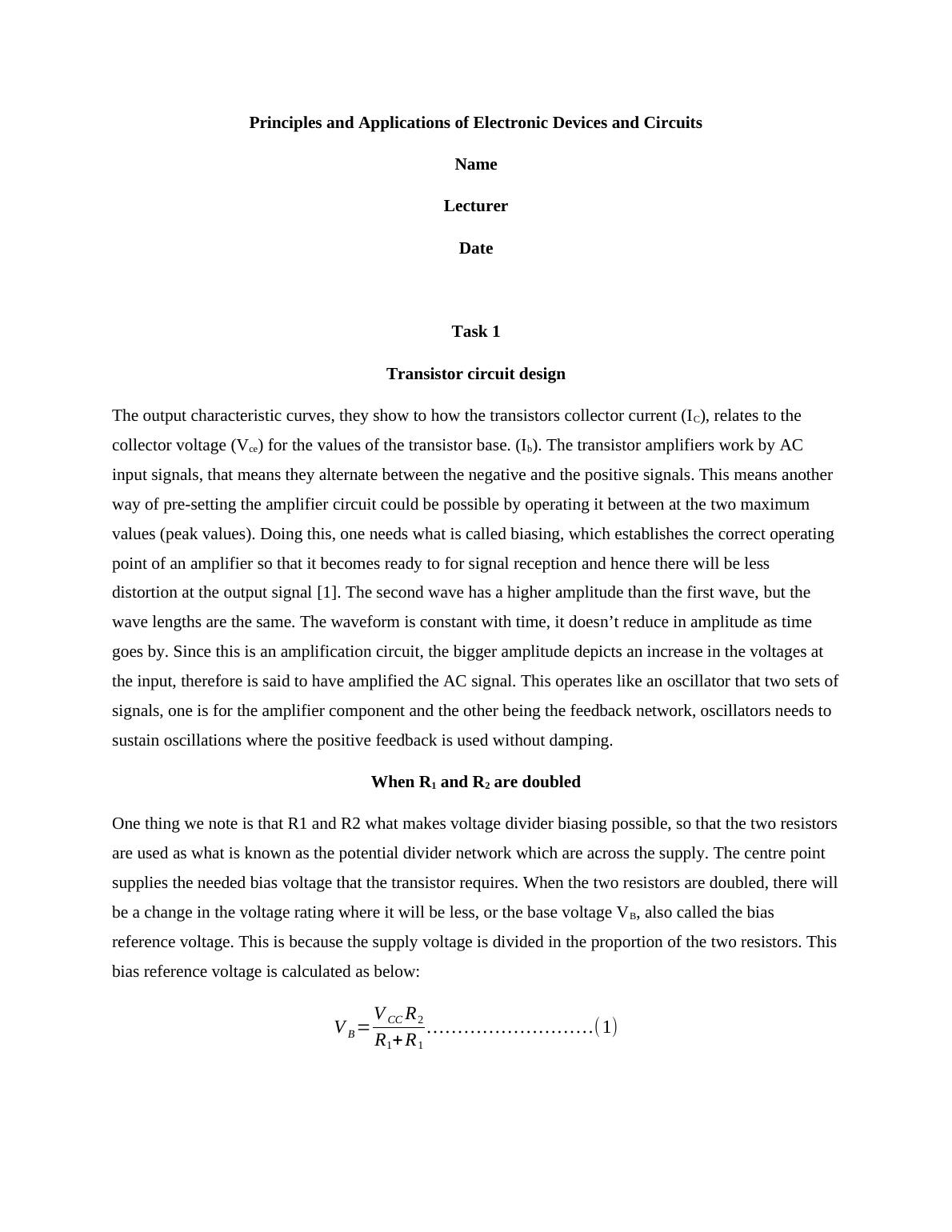
V B = V CC R2
R1+ R1
... ... ... ... ... ... ... ... ...( 1)

Also remember that the current at the junction will be less, this is because the collector voltage shall be
divided by the total resistance RT= R1+R2, which means the current I = VCC/RT
When R3 and R4 are halved
We know that for you to get the gain, you must consider the load voltage V Lor resistor and the input
voltage V B (where the base voltage in the input voltage and the load voltage being the output voltage) and
the voltage across the load or the emitter resistance. Simply put, the voltage is expressed as follows:
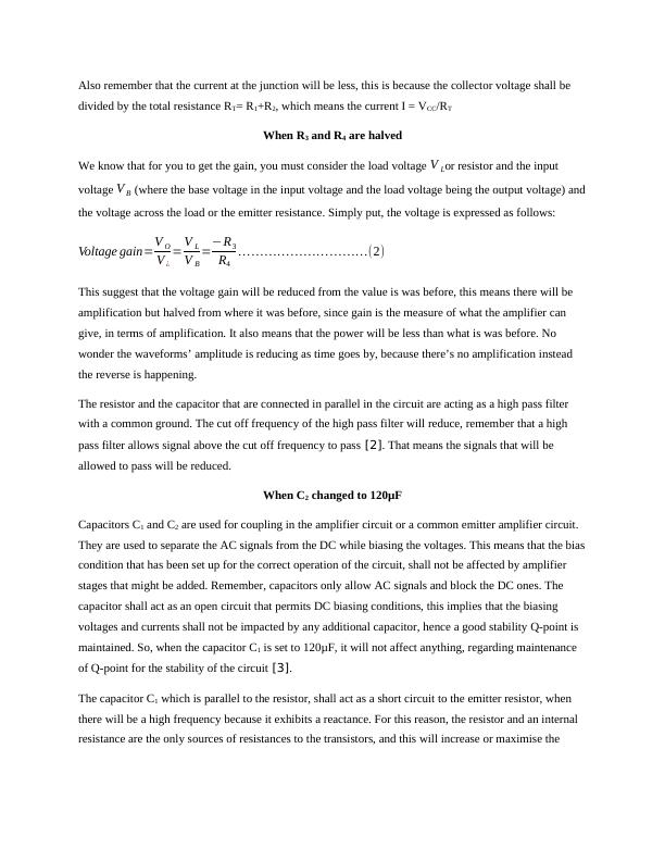
Voltage gain=V O
V ¿
= V L
V B
=−R3
R4
... ... ... ... ... ... ... ... ... ...(2)
This suggest that the voltage gain will be reduced from the value is was before, this means there will be
amplification but halved from where it was before, since gain is the measure of what the amplifier can
give, in terms of amplification. It also means that the power will be less than what is was before. No
wonder the waveforms’ amplitude is reducing as time goes by, because there’s no amplification instead
the reverse is happening.
The resistor and the capacitor that are connected in parallel in the circuit are acting as a high pass filter
with a common ground. The cut off frequency of the high pass filter will reduce, remember that a high
pass filter allows signal above the cut off frequency to pass [2]. That means the signals that will be
allowed to pass will be reduced.
When C2 changed to 120μF
Capacitors C1 and C2 are used for coupling in the amplifier circuit or a common emitter amplifier circuit.
They are used to separate the AC signals from the DC while biasing the voltages. This means that the bias
condition that has been set up for the correct operation of the circuit, shall not be affected by amplifier
stages that might be added. Remember, capacitors only allow AC signals and block the DC ones. The
capacitor shall act as an open circuit that permits DC biasing conditions, this implies that the biasing
voltages and currents shall not be impacted by any additional capacitor, hence a good stability Q-point is
maintained. So, when the capacitor C1 is set to 120μF, it will not affect anything, regarding maintenance
of Q-point for the stability of the circuit [3].
The capacitor C1 which is parallel to the resistor, shall act as a short circuit to the emitter resistor, when
there will be a high frequency because it exhibits a reactance. For this reason, the resistor and an internal
resistance are the only sources of resistances to the transistors, and this will increase or maximise the

End of preview
Want to access all the pages? Upload your documents or become a member.
Related Documents
Student. Professor. Principles and applications of Eleclg...
|17
|1906
|56
Amplifiers: Types, Characteristics and Performance Testslg...
|31
|3026
|131
Evolution of Electronics and Solid State Control Systemlg...
|10
|3707
|35
Power Amplifiers Design and Simulation | Reportlg...
|27
|3863
|37
DETERMINING THE CHARACTERISTICS OF THE AMPLIFIER CIRCUITSlg...
|29
|2706
|28
US03CPHY22 Unit 2 Small Signal Amplifierlg...
|19
|4202
|122
