Power Amplifiers Design and Simulation | Report
27 Pages3863 Words37 Views
Added on 2022-08-11
Power Amplifiers Design and Simulation | Report
Added on 2022-08-11
ShareRelated Documents
1
Student
Instructor
Title
POWER AMPLIFIERS DESIGN AND SIMULATION.
Date
Student
Instructor
Title
POWER AMPLIFIERS DESIGN AND SIMULATION.
Date
2
Table of Contents
1: INTRODUCTION.....................................................................................................................3
1.1: Finding Current Gain Ai.......................................................................................................5
1.2: Finding the Input Resistance.................................................................................................6
1.3: Finding Voltage Gain AV .....................................................................................................7
2: DESIGNING OF THE COMMON EMITTER POWER AMPLIFIER..............................9
2.1: Finding suitable collector load resistance of the circuit........................................................9
2.2: Finding the D.C operating point of the amplifier on the DC load line...............................10
2.3: Finding biasing resistor R1 and R2.....................................................................................15
2.4: Modification into Class B Amplifier..................................................................................18
2.5: Modification into Class AB Amplifier...............................................................................18
2.6: Modification into Class C Amplifier..................................................................................19
3: SIMULATION.........................................................................................................................21
4: RESULTS AND ANALYSIS..................................................................................................23
5: CONCLUSION........................................................................................................................25
6: REFERNCES...........................................................................................................................26
3
1: INTRODUCTION.
The project entails designing of class A amplifier using NPN transistor. The transistor naturally
operates as an amplifier in the active region where the collector current is linearly dependent on
the base current (ElProCus, 2020). Weak input signal at the base terminal of the transistor is
amplified when the base emitter junction of the transistor is forward biased. The polarity of the
input signal does not however, affects the biasing of the transistor (Tutorialspoint.com, 2018).
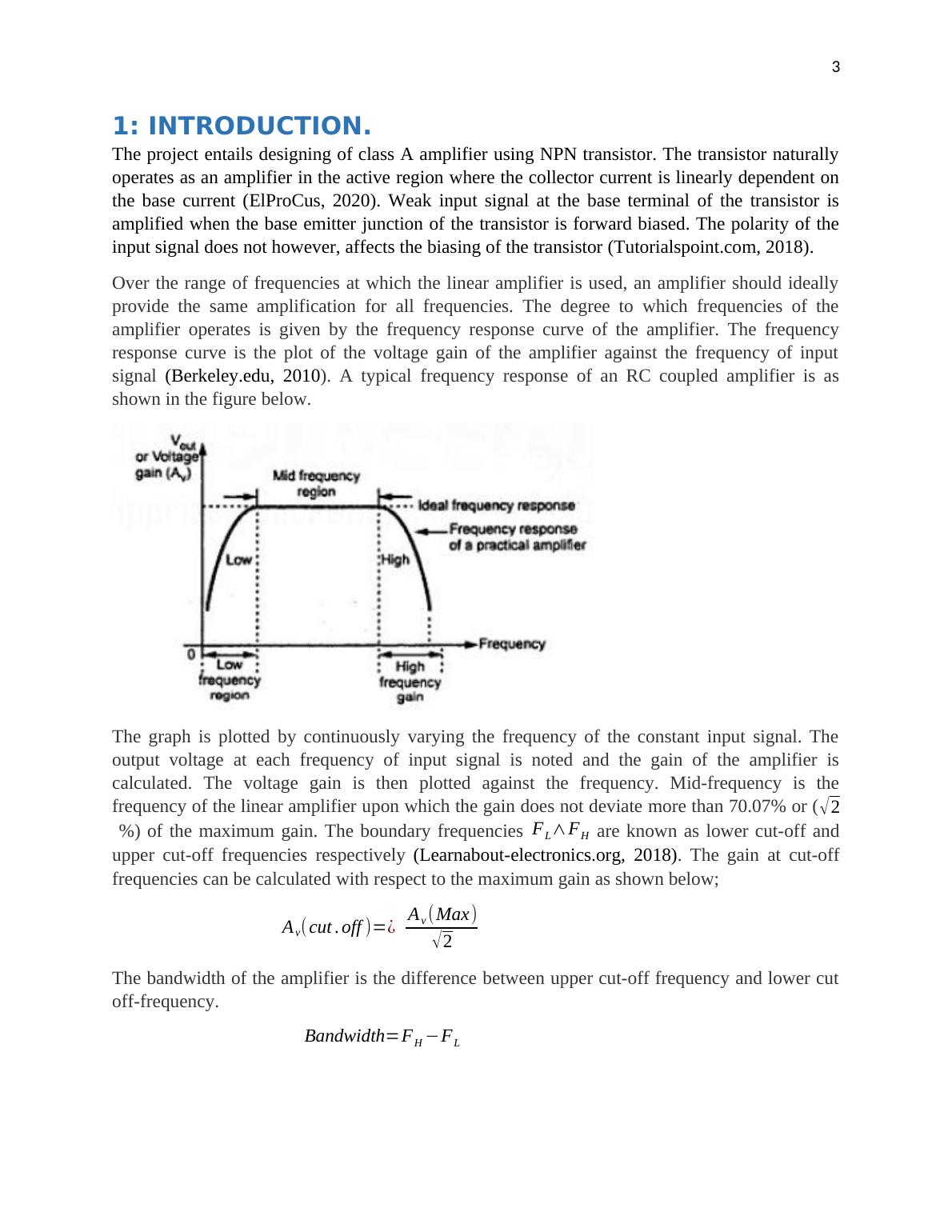
Over the range of frequencies at which the linear amplifier is used, an amplifier should ideally
provide the same amplification for all frequencies. The degree to which frequencies of the
amplifier operates is given by the frequency response curve of the amplifier. The frequency
response curve is the plot of the voltage gain of the amplifier against the frequency of input
signal (Berkeley.edu, 2010). A typical frequency response of an RC coupled amplifier is as
shown in the figure below.
The graph is plotted by continuously varying the frequency of the constant input signal. The
output voltage at each frequency of input signal is noted and the gain of the amplifier is
calculated. The voltage gain is then plotted against the frequency. Mid-frequency is the
frequency of the linear amplifier upon which the gain does not deviate more than 70.07% or ( √ 2
%) of the maximum gain. The boundary frequencies FL∧FH are known as lower cut-off and
upper cut-off frequencies respectively (Learnabout-electronics.org, 2018). The gain at cut-off
frequencies can be calculated with respect to the maximum gain as shown below;
Av(cut . off )=¿ Av (Max )
√2
The bandwidth of the amplifier is the difference between upper cut-off frequency and lower cut
off-frequency.
Bandwidth=FH −FL
1: INTRODUCTION.
The project entails designing of class A amplifier using NPN transistor. The transistor naturally
operates as an amplifier in the active region where the collector current is linearly dependent on
the base current (ElProCus, 2020). Weak input signal at the base terminal of the transistor is
amplified when the base emitter junction of the transistor is forward biased. The polarity of the
input signal does not however, affects the biasing of the transistor (Tutorialspoint.com, 2018).
Over the range of frequencies at which the linear amplifier is used, an amplifier should ideally
provide the same amplification for all frequencies. The degree to which frequencies of the
amplifier operates is given by the frequency response curve of the amplifier. The frequency
response curve is the plot of the voltage gain of the amplifier against the frequency of input
signal (Berkeley.edu, 2010). A typical frequency response of an RC coupled amplifier is as
shown in the figure below.
The graph is plotted by continuously varying the frequency of the constant input signal. The
output voltage at each frequency of input signal is noted and the gain of the amplifier is
calculated. The voltage gain is then plotted against the frequency. Mid-frequency is the
frequency of the linear amplifier upon which the gain does not deviate more than 70.07% or ( √ 2
%) of the maximum gain. The boundary frequencies FL∧FH are known as lower cut-off and
upper cut-off frequencies respectively (Learnabout-electronics.org, 2018). The gain at cut-off
frequencies can be calculated with respect to the maximum gain as shown below;
Av(cut . off )=¿ Av (Max )
√2
The bandwidth of the amplifier is the difference between upper cut-off frequency and lower cut
off-frequency.
Bandwidth=FH −FL
4
The amplifier amplifies properly within range of frequencies in the bandwidth. A good audio
amplifier must have bandwidth from 20 Hz to 20 kHz because that is the frequency range which
is audible.
The gain of the amplifier is the ratio of output power to input power. Gain can also be given by
the ratio of output voltage to input voltage as shown on the equation below.
Av=V out
V ¿
Or
Ap = Pout
P¿
Voltage gain of the amplifier can also be given in Decibels as shown in the expression below.
Voltage gain∈dB=20 log Av
Also, the power gain in Decibel is given by;
Power gain∈dB=10 log A p
When Av is greater than one, the dB gain is positive and when it is less than one, the dB gain is
negative. The negative and positive signs of dB indicate the amplification and attenuation
respectively.
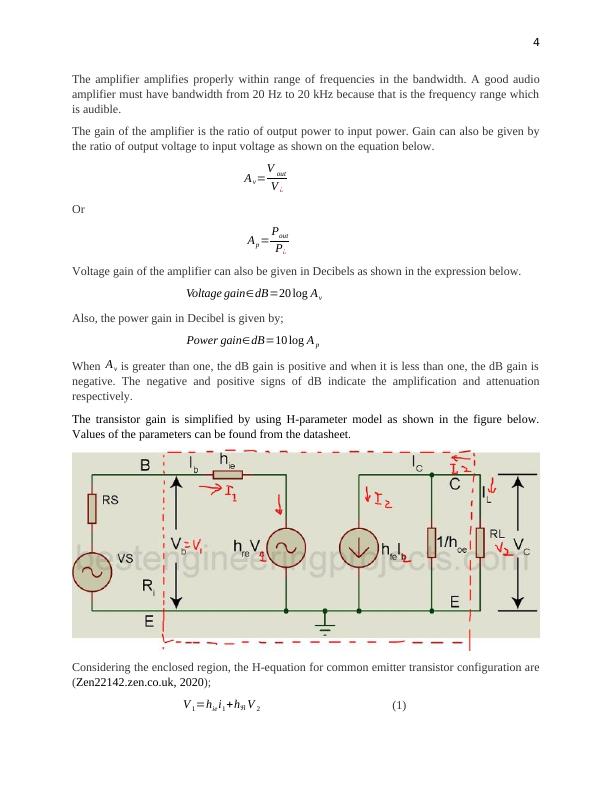
The transistor gain is simplified by using H-parameter model as shown in the figure below.
Values of the parameters can be found from the datasheet.
Considering the enclosed region, the H-equation for common emitter transistor configuration are
(Zen22142.zen.co.uk, 2020);
V 1=hie i1 +hℜ V 2 (1)
The amplifier amplifies properly within range of frequencies in the bandwidth. A good audio
amplifier must have bandwidth from 20 Hz to 20 kHz because that is the frequency range which
is audible.
The gain of the amplifier is the ratio of output power to input power. Gain can also be given by
the ratio of output voltage to input voltage as shown on the equation below.
Av=V out
V ¿
Or
Ap = Pout
P¿
Voltage gain of the amplifier can also be given in Decibels as shown in the expression below.
Voltage gain∈dB=20 log Av
Also, the power gain in Decibel is given by;
Power gain∈dB=10 log A p
When Av is greater than one, the dB gain is positive and when it is less than one, the dB gain is
negative. The negative and positive signs of dB indicate the amplification and attenuation
respectively.
The transistor gain is simplified by using H-parameter model as shown in the figure below.
Values of the parameters can be found from the datasheet.
Considering the enclosed region, the H-equation for common emitter transistor configuration are
(Zen22142.zen.co.uk, 2020);
V 1=hie i1 +hℜ V 2 (1)
5
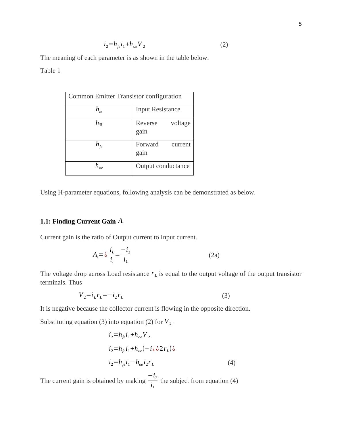
i2=hfei1 +hoeV 2 (2)
The meaning of each parameter is as shown in the table below.
Table 1
Common Emitter Transistor configuration
hie Input Resistance
hℜ Reverse voltage
gain
hfe Forward current
gain
hoe Output conductance
Using H-parameter equations, following analysis can be demonstrated as below.
1.1: Finding Current Gain Ai
Current gain is the ratio of Output current to Input current.
Ai=¿ iL
ii
=−i2
i1
(2a)
The voltage drop across Load resistance r L is equal to the output voltage of the output transistor
terminals. Thus
V 2=iL rL=−i2 rL (3)
It is negative because the collector current is flowing in the opposite direction.
Substituting equation (3) into equation (2) for V 2 .
i2=hfe i1 +hoe V 2
i2=hfe i1 +hoe (−i ¿¿ 2 rL)¿
i2=hfe i1−hoe i2 r L (4)
The current gain is obtained by making −i2
i1
the subject from equation (4)
6
i2+ hoe i2 r L=hfe i1
i2 ( 1+ hoe r L ) =hfe i1
i2
i1
= hfe
( 1+hoe r L ) (5)
But from the current gain in expression (2a), the current gain is given by;
Ai=−i2
i1
= −hfe
( 1+ hoe r L ) (6)
Equation (6) is the current gain expression.
1.2: Finding the Input Resistance
This is the resistance looking into the input of the amplifier terminals (1,1’). It is also called
Input Resistance looking into the base ( R¿ base)
R¿ base= V 1
i1
(7)
Substituting the values of V 2 as from equation (3) into equation (1).
V 1=hie i1 +hℜ V 2
V 1=hie i1 +hℜ(−i¿ ¿2 r L)¿
V 1=hie i1−hℜ i2 rL (8)
Dividing equation (8) through by i1
V 1
i1
=hie− hℜ i2 r L
i1
(9)
But from current gain of equation (6)
Ai=−i2
i1
= −hfe
( 1+ hoe r L ) (10)
Substituting into equation (9), the expression becomes
V 1
i1
=hie−hℜ rL { hfe
( 1+ hoe r L ) } (11)
End of preview
Want to access all the pages? Upload your documents or become a member.
Related Documents
Designing an Audio Amplifier: Steps and Analysislg...
|13
|2054
|268
DETERMINING THE CHARACTERISTICS OF THE AMPLIFIER CIRCUITSlg...
|29
|2706
|28
Principles and Applications of Electronic Devices and Circuitslg...
|4
|1212
|69
Evolution of Electronics and Solid State Control Systemlg...
|10
|3707
|35
Amplifier Circuits: Types, Characteristics and Applicationslg...
|19
|1241
|288
Design of Multistage Operational Amplifierlg...
|17
|5051
|59