logo

Electronic Circuits and Devices: Operational Amplifiers, Feedback Circuits, and Oscillators

This assignment is about amplifier circuits and applications in the field of electronic circuits and devices. The assignment requires the students to determine the operational characteristics of amplifier circuits, investigate the types and effects of feedback on an amplifier's performance, and examine the operation and application of oscillators. The assignment should be submitted in the form of a report, showing all work in a neat and organized manner. The experimental part of the assignment requires students to reserve lab time with Eng. Nadia ahead of time to complete tests.

28 Pages3986 Words465 Views
   

Added on  2023-04-22

About This Document

This document discusses the comparison between different types of operational amplifiers, feedback circuits, and oscillators. It includes circuit diagrams, simulations, and analysis of the performance of different circuits. The document is relevant for students studying electronic circuits and devices in college or university.

Electronic Circuits and Devices: Operational Amplifiers, Feedback Circuits, and Oscillators

This assignment is about amplifier circuits and applications in the field of electronic circuits and devices. The assignment requires the students to determine the operational characteristics of amplifier circuits, investigate the types and effects of feedback on an amplifier's performance, and examine the operation and application of oscillators. The assignment should be submitted in the form of a report, showing all work in a neat and organized manner. The experimental part of the assignment requires students to reserve lab time with Eng. Nadia ahead of time to complete tests.

   Added on 2023-04-22

ShareRelated Documents
Running head: ELECTRONIC CIRCUITS AND DEVICES
ELECTRONIC CIRCUITS AND DEVICES
Name of the Student
Name of the University
Author Note
Electronic Circuits and Devices: Operational Amplifiers, Feedback Circuits, and Oscillators_1
1ELECTRONIC CIRCUITS AND DEVICES
Scenario 1:
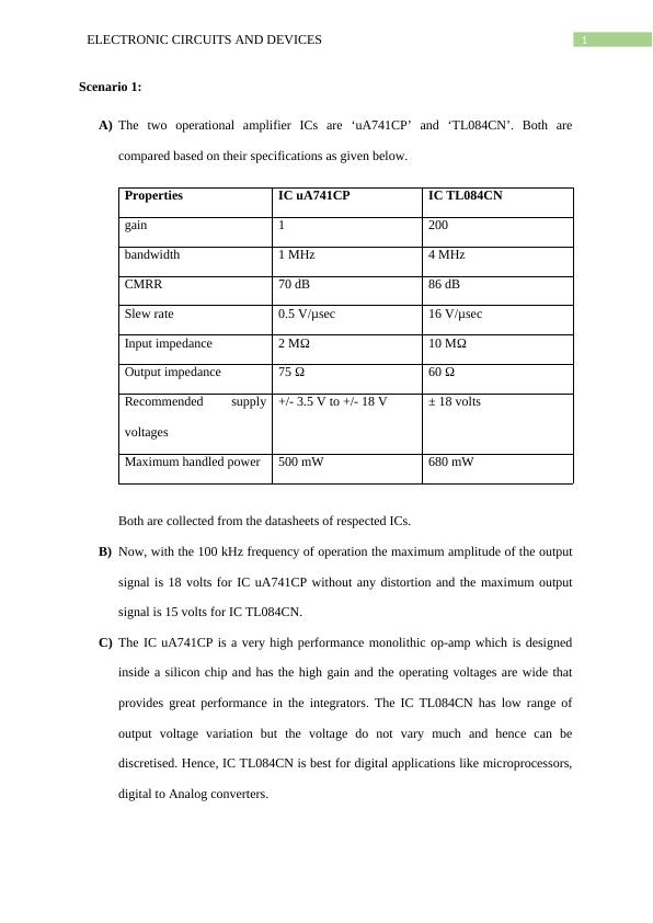
A) The two operational amplifier ICs are ‘uA741CP’ and ‘TL084CN’. Both are
compared based on their specifications as given below.
Properties IC uA741CP IC TL084CN
gain 1 200
bandwidth 1 MHz 4 MHz
CMRR 70 dB 86 dB
Slew rate 0.5 V/μsec 16 V/μsec
Input impedance 2 MΩ 10 MΩ
Output impedance 75 Ω 60 Ω
Recommended supply
voltages
+/- 3.5 V to +/- 18 V ± 18 volts
Maximum handled power 500 mW 680 mW
Both are collected from the datasheets of respected ICs.
B) Now, with the 100 kHz frequency of operation the maximum amplitude of the output
signal is 18 volts for IC uA741CP without any distortion and the maximum output
signal is 15 volts for IC TL084CN.
C) The IC uA741CP is a very high performance monolithic op-amp which is designed
inside a silicon chip and has the high gain and the operating voltages are wide that
provides great performance in the integrators. The IC TL084CN has low range of
output voltage variation but the voltage do not vary much and hence can be
discretised. Hence, IC TL084CN is best for digital applications like microprocessors,
digital to Analog converters.
Electronic Circuits and Devices: Operational Amplifiers, Feedback Circuits, and Oscillators_2
2ELECTRONIC CIRCUITS AND DEVICES
D) The op-amp IC that is most suitable for instrumental amplifier application needs to be
suitable for Analog applications. Hence, as IC uA741CP is most suitable for Analog
applications hence IC uA741CP is the most suitable operation amplifier.’
E) Given that the 2 kHz input signal has been amplified to 20 Volt peak to peak by the
use of the inverting op-amp circuit. Now, the op-amp needs to be amplified even more
so that the 20 Ω load of 50 Volt peak to peak can be fed. Now, two power amplifiers
either class A or class B is used for amplification.
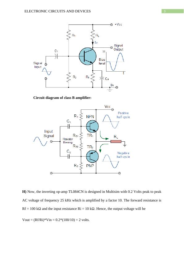
Now, the advantages of class B amplifier are the bias current is very low. Hence, the
power consumption is negligible. Class B amplifiers can be effectively used for high
level output than the class A. Thus class B is more efficient than class A (Pedro and
Cabral 2015). There are a few disadvantages of the class B amplifier like crossover
distortion is created, the supply current is not constant but it is changing with signal
and hence a stabilized supply is needed.
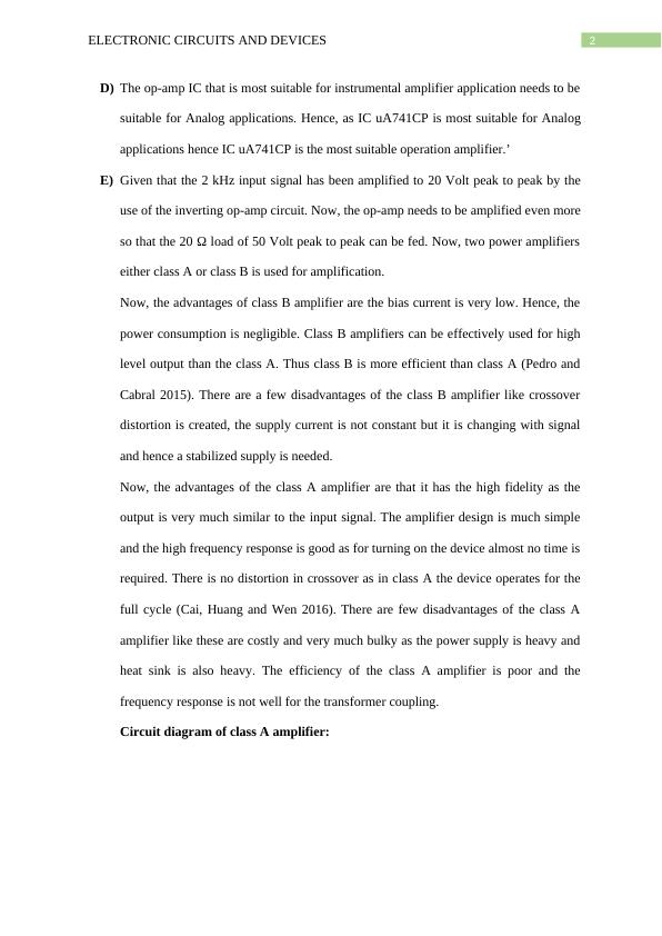
Now, the advantages of the class A amplifier are that it has the high fidelity as the
output is very much similar to the input signal. The amplifier design is much simple
and the high frequency response is good as for turning on the device almost no time is
required. There is no distortion in crossover as in class A the device operates for the
full cycle (Cai, Huang and Wen 2016). There are few disadvantages of the class A
amplifier like these are costly and very much bulky as the power supply is heavy and
heat sink is also heavy. The efficiency of the class A amplifier is poor and the
frequency response is not well for the transformer coupling.
Circuit diagram of class A amplifier:
Electronic Circuits and Devices: Operational Amplifiers, Feedback Circuits, and Oscillators_3
3ELECTRONIC CIRCUITS AND DEVICES
Circuit diagram of class B amplifier:
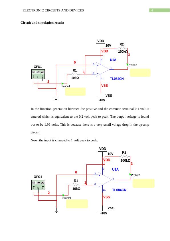
H) Now, the inverting op-amp TL084CN is designed in Multisim with 0.2 Volts peak to peak
AC voltage of frequency 25 kHz which is amplified by a factor 10. The forward resistance is
Rf = 100 kΩ and the input resistance Ri = 10 kΩ. Hence, the output voltage will be
Vout = (Rf/Ri)*Vin = 0.2*(100/10) = 2 volts.
Electronic Circuits and Devices: Operational Amplifiers, Feedback Circuits, and Oscillators_4
4ELECTRONIC CIRCUITS AND DEVICES
Circuit and simulation result:
U1A
TL084CN
3
2
11
4
1
R1
10kΩ
XFG1
VDD
10V
VSS
-10V
VDD
VSS
R2
100kΩ
1
3
0
2
Probe2
V(p-p): 1.99 V
Freq.: 25.0 kHz
Probe1
V(p-p): 200 mV
Freq.: 25.0 kHz
In the function generation between the positive and the common terminal 0.1 volt is
entered which is equivalent to the 0.2 volt peak to peak. The output voltage is found
out to be 1.99 volts. This is because there is a very small volage drop in the op-amp
circuit.
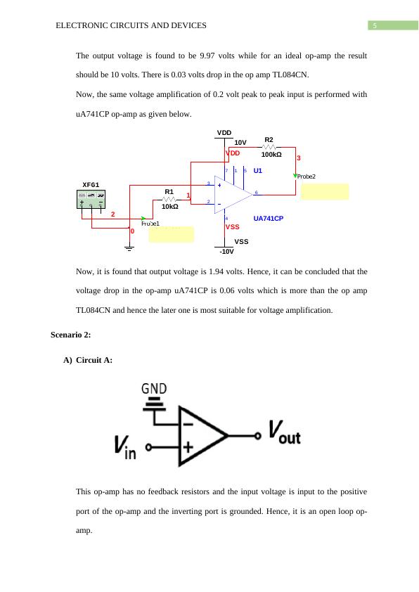
Now, the input is changed to 1 volt peak to peak.
U1A
TL084CN
3
2
11
4
1
R1
10kΩ
XFG1
VDD
10V
VSS
-10V
VDD
VSS
R2
100kΩ
1
3
0
2
Probe2
V(p-p): 9.97 V
Freq.: 25.0 kHz
Probe1
V(p-p): 1.00 V
Freq.: 25.0 kHz
Electronic Circuits and Devices: Operational Amplifiers, Feedback Circuits, and Oscillators_5
5ELECTRONIC CIRCUITS AND DEVICES
The output voltage is found to be 9.97 volts while for an ideal op-amp the result
should be 10 volts. There is 0.03 volts drop in the op amp TL084CN.
Now, the same voltage amplification of 0.2 volt peak to peak input is performed with
uA741CP op-amp as given below.
R1
10kΩ
XFG1
VDD
10V
VSS
-10V
R2
100kΩ
2
U1
UA741CP
3
2
4
7
6
51
VSS
1
0
3
VDD
Probe1
V(p-p): 200 mV
Freq.: 25.0 kHz
Probe2
V(p-p): 1.94 V
Freq.: 25.0 kHz
Now, it is found that output voltage is 1.94 volts. Hence, it can be concluded that the
voltage drop in the op-amp uA741CP is 0.06 volts which is more than the op amp
TL084CN and hence the later one is most suitable for voltage amplification.
Scenario 2:
A) Circuit A:
This op-amp has no feedback resistors and the input voltage is input to the positive
port of the op-amp and the inverting port is grounded. Hence, it is an open loop op-
amp.
Electronic Circuits and Devices: Operational Amplifiers, Feedback Circuits, and Oscillators_6

End of preview

Want to access all the pages? Upload your documents or become a member.

Related Documents
Measurement & Evaluation of Audio Amplifier Circuit Assignment PDF
|9
|1695
|501

Implementation of 4-bit DAC converter using R-2R resistor ladder
|6
|837
|151

Electrical and Electronic Principles: Sensor Circuit Design, Logic Design, and A.C. Load Supply
|6
|737
|256

Electrical and Electronic Principles: Sensor Circuit Design, Logic Design, and A.C. Load Supply
|7
|766
|321

Power Amplifier PAE Components: Classification and Application
|6
|3234
|53

An analogue quantities are those quantities
|10
|1933
|19