Digital Electronics: IEEE 754, Flip-Flops, and Logic Circuits
VerifiedAdded on 2023/01/04
|12
|1995
|3
Homework Assignment
AI Summary
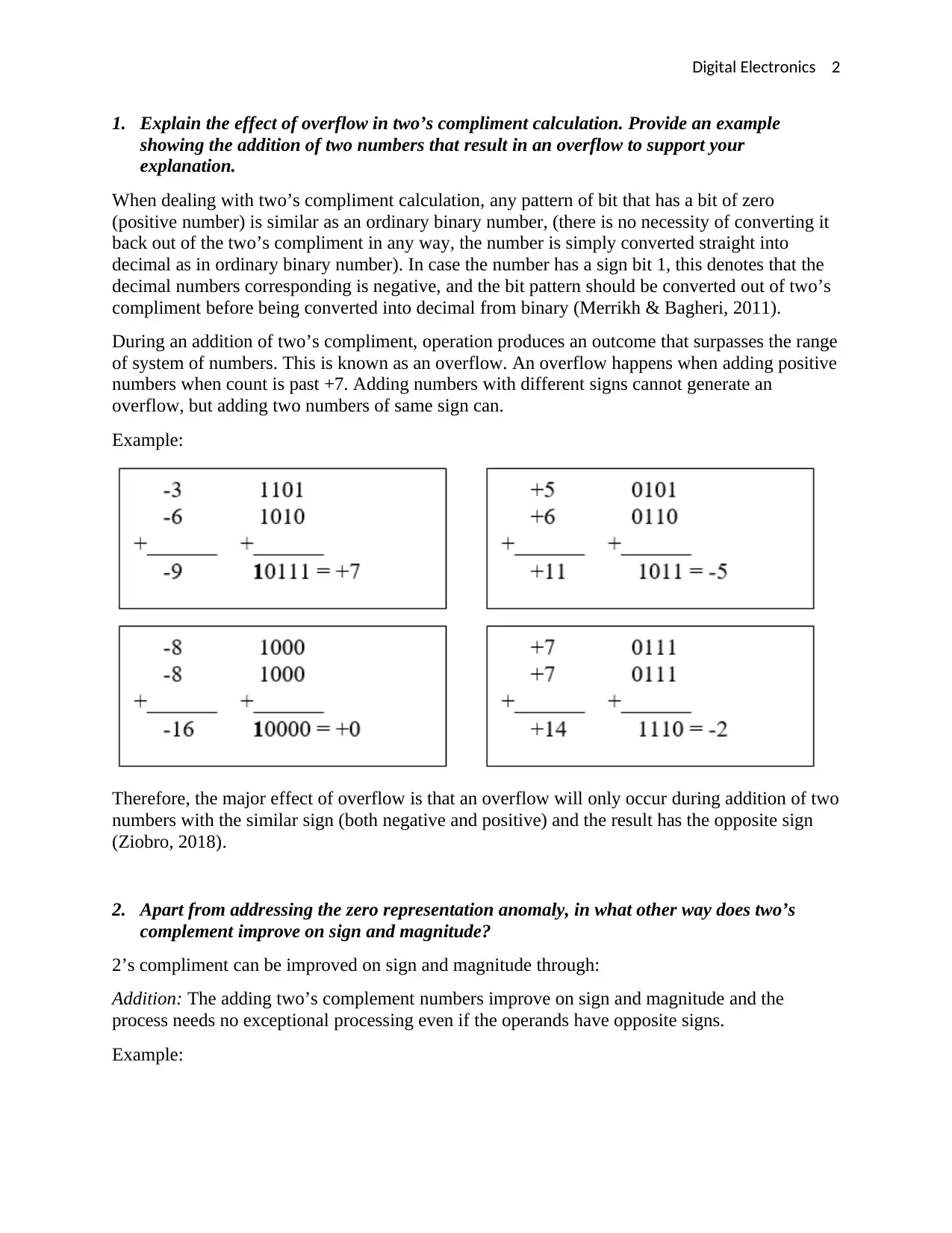
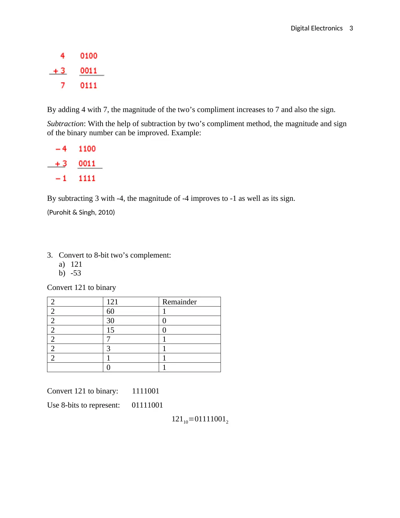
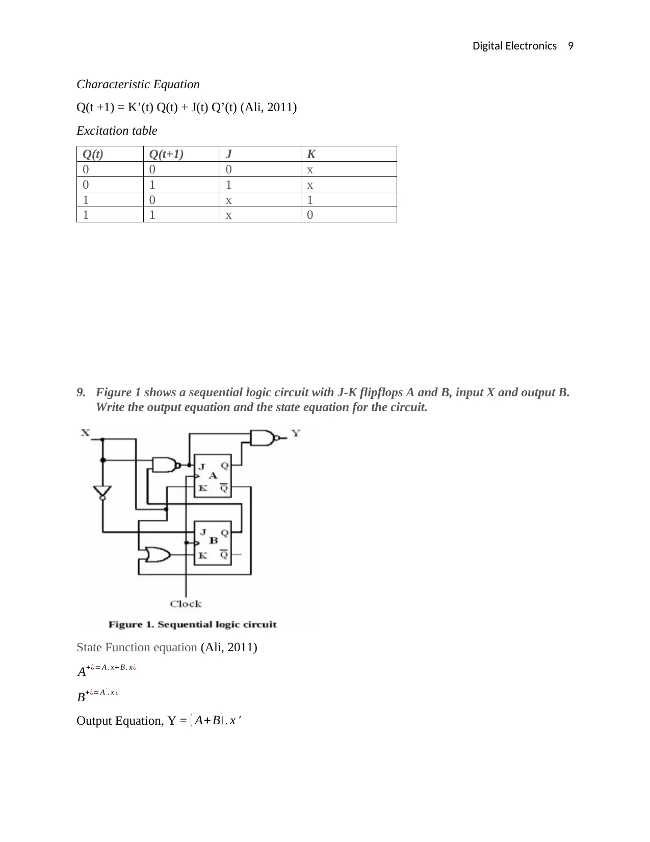
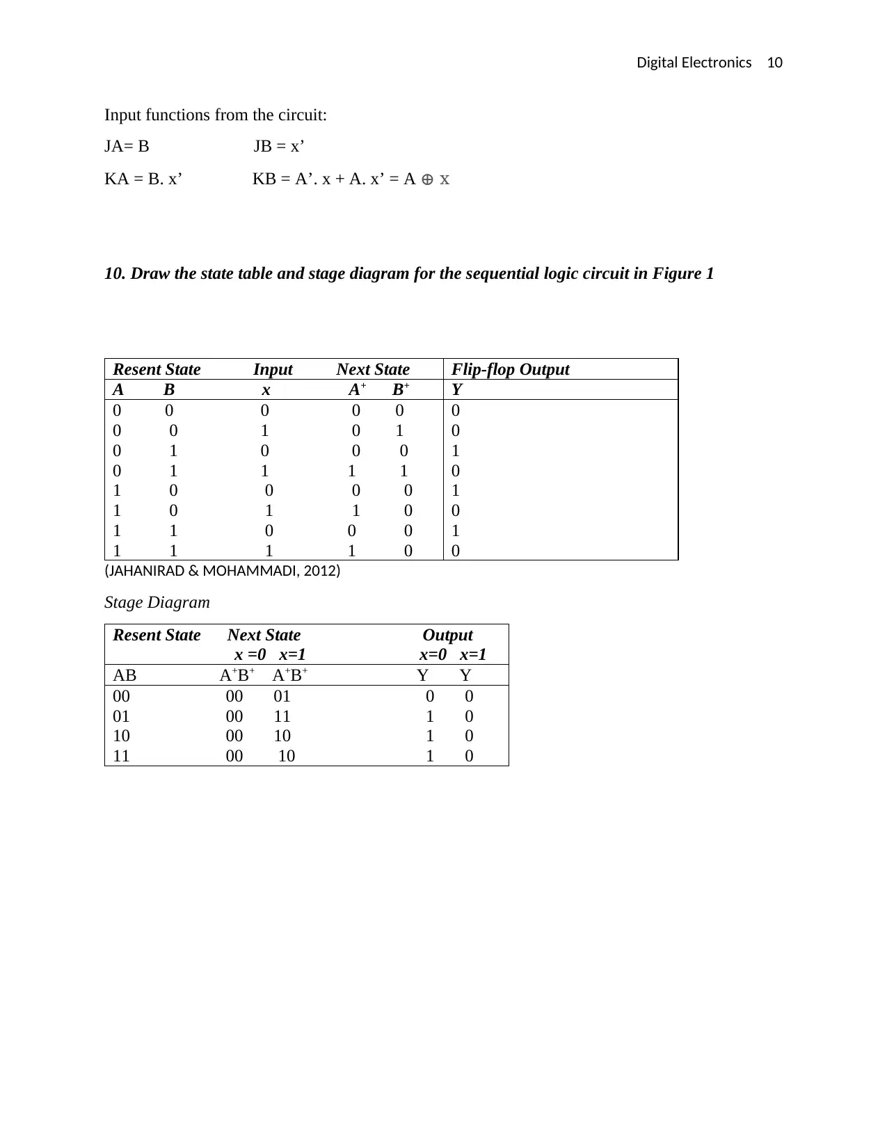
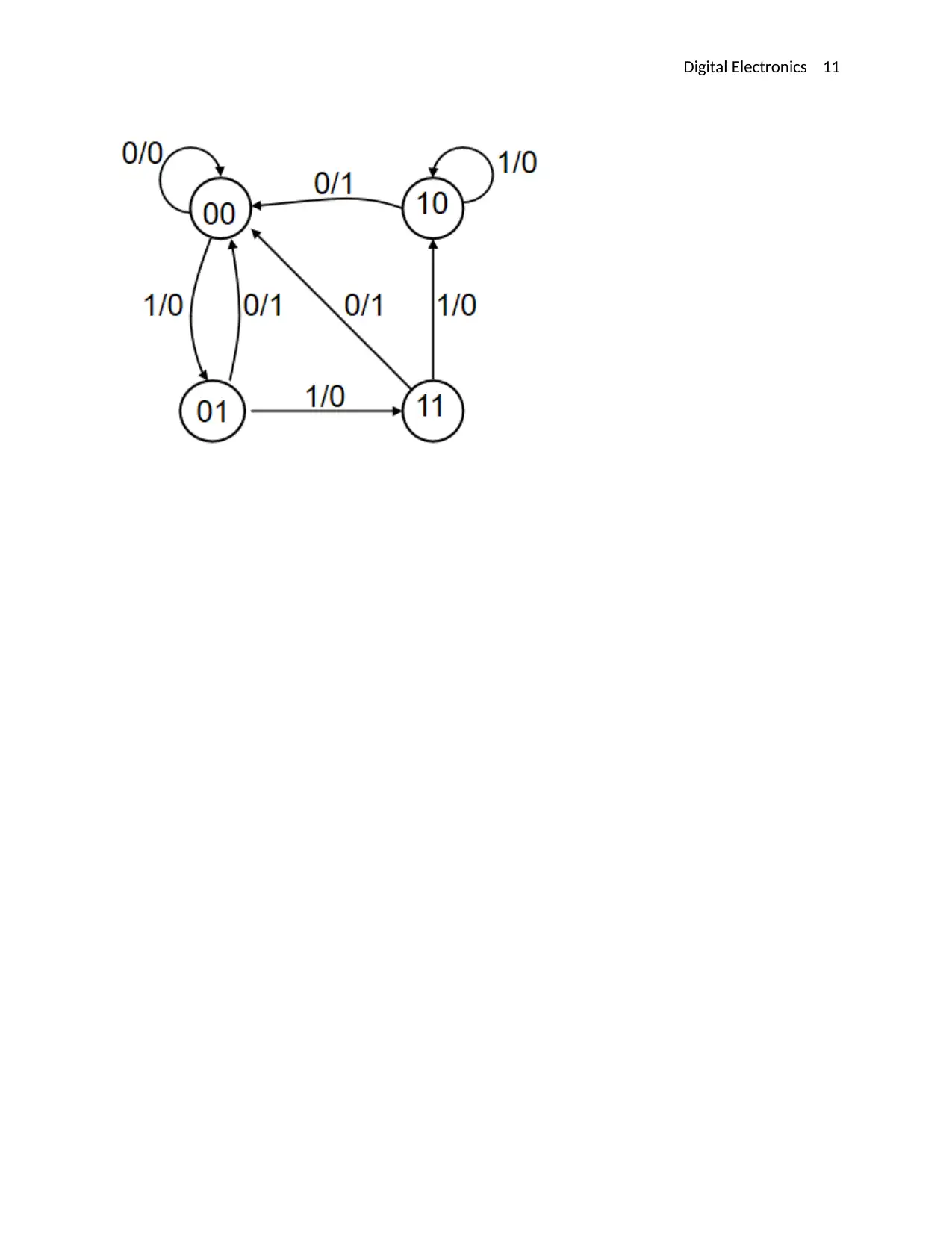
This document provides a comprehensive solution to a digital electronics assignment, covering key concepts in computer architecture and design. The solution begins by explaining the effects of overflow in two's complement calculations, providing examples to illustrate the concept. It then compares and contrasts two's complement with sign and magnitude representations, highlighting the improvements in addition and subtraction operations. The assignment includes detailed conversions of decimal numbers to 8-bit two's complement and vice versa. Furthermore, the solution explains the IEEE 754 approach for representing single-precision floating-point numbers, with diagrams illustrating the format. The document also includes diagrams and explanations for constructing a two's complement adder/subtractor using a 4-bit full adder and controlled inverter. Finally, the assignment addresses the characteristics and excitation tables for T and JK flip-flops, along with the output and state equations, state tables, and state diagrams for a given sequential logic circuit. The document concludes with a bibliography of the cited sources.

Digital Electronics 1
COMPUTER ARCHITECTURE AND DESIGN
By Name
Course
Instructor
Institution
Location
Date
COMPUTER ARCHITECTURE AND DESIGN
By Name
Course
Instructor
Institution
Location
Date
Paraphrase This Document
Need a fresh take? Get an instant paraphrase of this document with our AI Paraphraser

Digital Electronics 2
1. Explain the effect of overflow in two’s compliment calculation. Provide an example
showing the addition of two numbers that result in an overflow to support your
explanation.
When dealing with two’s compliment calculation, any pattern of bit that has a bit of zero
(positive number) is similar as an ordinary binary number, (there is no necessity of converting it
back out of the two’s compliment in any way, the number is simply converted straight into
decimal as in ordinary binary number). In case the number has a sign bit 1, this denotes that the
decimal numbers corresponding is negative, and the bit pattern should be converted out of two’s
compliment before being converted into decimal from binary (Merrikh & Bagheri, 2011).
During an addition of two’s compliment, operation produces an outcome that surpasses the range
of system of numbers. This is known as an overflow. An overflow happens when adding positive
numbers when count is past +7. Adding numbers with different signs cannot generate an
overflow, but adding two numbers of same sign can.
Example:
Therefore, the major effect of overflow is that an overflow will only occur during addition of two
numbers with the similar sign (both negative and positive) and the result has the opposite sign
(Ziobro, 2018).
2. Apart from addressing the zero representation anomaly, in what other way does two’s
complement improve on sign and magnitude?
2’s compliment can be improved on sign and magnitude through:
Addition: The adding two’s complement numbers improve on sign and magnitude and the
process needs no exceptional processing even if the operands have opposite signs.
Example:

Digital Electronics 3
By adding 4 with 7, the magnitude of the two’s compliment increases to 7 and also the sign.
Subtraction: With the help of subtraction by two’s compliment method, the magnitude and sign
of the binary number can be improved. Example:
By subtracting 3 with -4, the magnitude of -4 improves to -1 as well as its sign.
(Purohit & Singh, 2010)
3. Convert to 8-bit two’s complement:
a) 121
b) -53
Convert 121 to binary
2 121 Remainder
2 60 1
2 30 0
2 15 0
2 7 1
2 3 1
2 1 1
0 1
Convert 121 to binary: 1111001
Use 8-bits to represent: 01111001
12110=011110012
⊘ This is a preview!⊘
Do you want full access?
Subscribe today to unlock all pages.

Trusted by 1+ million students worldwide

Digital Electronics 4
-53
2 53 Remainder
2 26 1
2 13 0
2 6 1
2 3 0
2 1 1
0 1
Convert -53 to binary: 110101
Use 8-bit to represent: 00110101
Change to negative: 10110101
−5310=101101012
4. Convert the following two’s complement numbers to decimal:
a) 1101 1001
b) 0110 0010
Two’s complement = 1101 1001
Complement = 00100110
Add 1 +1
True binary = 0010 0111
Decimal equivalent = 27
b) 0110 0010
Two’s complement = 0110 0010
Complement = 1001 1101
Decimal equivalent = 9D
(Chattopadhyay & Kumar, 2017)
Paraphrase This Document
Need a fresh take? Get an instant paraphrase of this document with our AI Paraphraser

Digital Electronics 5
5. With the help of a diagram, explain how the IEEE 754 approach represents single
precision floating point numbers
The most common representation is IEEE 754 floating point currently on computers for real
numbers, including most Unix platforms, Macintoshes, and intel-based PC’s. Precision floating
point number is a format of computer number, normally occupying 32-bits in computer memory
for single precision and 64-bit for double precision (Yueh, et al., 2011).
The maximum value of an IEEE 754 32-bit floating point variable is (2 − 2−23) × 2127 ≈
3.4028235 × 1038, whereas the maximum value of a signed 32-bit integer variable is 231 − 1 =
2,147,483,647.
The Smallest value:
Largest value:
The number is determined by the sign bit, which is also the significand sign. Exponent may be an
8-bit unsigned integer from 0 to 255 or an 8-bit signed integer from -128 to 127, which is the
recognized biased definition of IEEE 754 binary32. The correct significand entails implicit
leading bit with value 1 and 23 fraction bits to the binary point right side.

Digital Electronics 6
6. Draw a diagram to show how the number -56.25 is represented in the IEEE754 single
precision floating point number representation.
Represent -56.25
Fraction part = 0.25
-0.25 x 2 = -0.500 → b−1=0
-0.500 x 2 = -1.000 = -1 + 0.000 → b−2=−1, fraction=0.000 , terminate
Therefore, (0.25)10 can be represented in binary as (-0.001)2
Normalized binary scientific notation; -1.0 x 2-3
2 56 Remainder
2 28 0
2 14 0
2 7 0
2 3 1
2 1 1
0 1
Convert 56 to binary: 00111000
Convert -56 to binary = 10111000
Therefore, (-56.25)10 = (-56)10 + (-0.25)10 = (10111000)10 + (-0.001)2
(-56.25)10 = 101110002 = (1.0111)2 x 2-6
Exponential = -6 and biased form is therefore 130 = 1000 0010
The resulting 32 bit IEEE 754 binary32 format -56.25 representation as 0-10111000-1000
00100000000 = 41460000H
(Yueh, et al., 2011)
⊘ This is a preview!⊘
Do you want full access?
Subscribe today to unlock all pages.

Trusted by 1+ million students worldwide

Digital Electronics 7
7. With the help of a diagram, explain how a two’s complement adder/subtractor can be
created by combining a 4-bit full adder with a controlled inverter.
A 4-bit adder using full adder circuits has the ability tow 4-bit numbers resulting in a carry
output and a 4-bit numbers. The subtraction of two binary numbers may be attained through
taking two’s complement of the subtrahend and adding to the minuend. Through this procedure,
the subtraction changes to addition operation. The input can be controlled in controlled inverter
as per the requirements and hence controlling the subtraction and addition using two’s
complement method in parallel binary full subtractor/adder circuit. In a 4-bit adder circuit a
single input of 4 XOR gates of controlled inverter are maintained constant in 1 and 0 at the time
of subtraction or addition respectively (Mukherjee, 2014).
The XOR gate passes another input of the gate directly to the adder and the addition operation
takes place in case of addition as one XOR gate input and the carry in bit of 1st full adder as in
active low condition (0).
The XOR gate passes the 2’s complement of another input and then addition takes place together
with carry-in bit in case of subtraction as one of the input as in active high condition (1).
Therefore, the input if controlled inverted. The controlled inverter together with the four-bit
parallel adder constitute the four-bit subtractor/adder composite unit (Mukherjee, 2011).
Paraphrase This Document
Need a fresh take? Get an instant paraphrase of this document with our AI Paraphraser

Digital Electronics 8
8. a) Write the characteristic equation and the excitation table for the T flip-flop.
Truth table
T Q(t +1)
0 Q(t)
1 Q’(t)
Characteristic Equation
Q(t +1) = T’(t) Q(t) + T(t) Q’(t) = T(t) ⊕ Q(t) (Ali, 2011)
Excitation Table
Q(t) Q(t+1) T
0 0 0
0 1 1
1 0 1
1 1 0
b. Write the characteristic equation and the excitation table for the J-K flip-flop
Truth Table
J K Q(t+1)
0 0 Q(t)
0 1 0
1 0 1
1 1 Q’(t)

Digital Electronics 9
Characteristic Equation
Q(t +1) = K’(t) Q(t) + J(t) Q’(t) (Ali, 2011)
Excitation table
Q(t) Q(t+1) J K
0 0 0 x
0 1 1 x
1 0 x 1
1 1 x 0
9. Figure 1 shows a sequential logic circuit with J-K flipflops A and B, input X and output B.
Write the output equation and the state equation for the circuit.
State Function equation (Ali, 2011)
A+¿= A . x+ B . x¿
B+¿= A ' . x ¿
Output Equation, Y = ( A+ B ) . x '
⊘ This is a preview!⊘
Do you want full access?
Subscribe today to unlock all pages.

Trusted by 1+ million students worldwide

Digital Electronics 10
Input functions from the circuit:
JA= B JB = x’
KA = B. x’ KB = A’. x + A. x’ = A ⊕ x
10. Draw the state table and stage diagram for the sequential logic circuit in Figure 1
Resent State Input Next State Flip-flop Output
A B x A+ B+ Y
0 0 0 0 0
0 0 1 0 1
0 1 0 0 0
0 1 1 1 1
1 0 0 0 0
1 0 1 1 0
1 1 0 0 0
1 1 1 1 0
0
0
1
0
1
0
1
0
(JAHANIRAD & MOHAMMADI, 2012)
Stage Diagram
Resent State Next State Output
x =0 x=1 x=0 x=1
AB A+B+ A+B+ Y Y
00 00 01 0 0
01 00 11 1 0
10 00 10 1 0
11 00 10 1 0
Paraphrase This Document
Need a fresh take? Get an instant paraphrase of this document with our AI Paraphraser

Digital Electronics 11

Digital Electronics 12
BIBLIOGRAPHY
Ali, B., 2011. Design of Reversible Sequential Circuit Using Reversible Logic Synthesis. s.l.:International
Journal of VLSI Design & Communication Systems. Vol 2. pp. 37-45.
Chattopadhyay, T. & Kumar, D., 2017. All-optical 2's complement number conversion scheme without
binary addition. s.l.:IET Optoelectronics. Vol 11. pp. 1-7.
JAHANIRAD, H. & MOHAMMADI, K., 2012. SEQUENTIAL LOGIC CIRCUITS RELIABILITY ANALYSIS.
s.l.:Journal of Circuits, Systems and Computers. Vol 21. pp. 125.
Merrikh, F. & Bagheri, S., 2011. Memristor-based circuits for performing basic arithmetic operations.
s.l.:Procedia Computer Science. Vol 3. pp. 128-132.
Mukherjee, K., 2011. Method of implementation of frequency encoded all optical half adder, half
subtractor and full adder based on semiconductor optical amplifiers and add drop multiplexers. s.l.:Optik.
Vol 122. pp. 1188-1194.
Mukherjee, K., 2014. Frequency encoded optical four-bit adder/subtractor with control input using
semiconductor optical amplifiers. s.l.:Optik. Vol 125. pp. 6183-6188.
Purohit, G. & Singh, A., 2010. Efficient Implementation of Arithmetic Operations in ECC over Binary
Fields. s.l.:International Journal of Computer Applications. Vol 6. pp. 5-9.
Yueh, C., Yang, C., Yang, C. & Hong, C., 2011. Arithmetic operations beyond floating point number
precision. s.l.:International Journal of Computational Science and Engineering. Vol 6. pp. 206.
Ziobro, R., 2018. Arithmetic Operations on Short Finite Sequences. s.l.:Formalized Mathematics. Vol 26.
pp. 199-208.
⊘ This is a preview!⊘
Do you want full access?
Subscribe today to unlock all pages.

Trusted by 1+ million students worldwide
1 out of 12
Related Documents
Your All-in-One AI-Powered Toolkit for Academic Success.
+13062052269
info@desklib.com
Available 24*7 on WhatsApp / Email
Unlock your academic potential
Copyright © 2020–2025 A2Z Services. All Rights Reserved. Developed and managed by ZUCOL.


