Designing variable output power supply Project 2022
Added on 2022-09-22
30 Pages3868 Words26 Views

Summary
The objectives of the project were to design and simulate a variable output power supply. The
variable output was then used to control the speed of a constant load permanent magnet DC
motor. The variable output power supply was accomplished using two design techniques;
MOSFET and BJT based power supply. A capacitor smoothed full bridge rectifier circuit that
converts low voltage AC to DC was designed to produce an unregulated voltage of 12 volts. The
unregulated output voltage from the rectifier was then regulated using either using an IC
regulator circuit or feedback stabilized voltage regulator. Both feedback stabilized voltage
regulators, and the IC regulator was designed to produce a variable, regulated output voltage
ranging from 5 to 10 volts. The circuit was tested to ascertain the voltage range at the output of
each power supply technique. The MOSFET based power supply produced a wide range of
output voltage, but our interest was 5-10 volts. The variable output was then used to power the
DC motor. The speed of a motor increases as the input voltages are increased.
2
List of contents
1.0 Introduction.................................................................................................4
2.0 Circuit design...............................................................................................5
2.1 Rectifier design....................................................................................5
2.2 Smoothing capacitor design.....................................................................6
2.3 Voltage regulation................................................................................7
2.3.1 Feedback stabilized variable regulator............................................7
2.3.2 Integrated circuit voltage regulator..............................................10
3.0 Circuit simulations.......................................................................................12
3.1 Rectifier simulation.............................................................................12
3.2 Regulator simulation...........................................................................14
3.2.1 IC regulator circuit.................................................................14
3.2.2 Screenshots of IC regulator voltage readings..................................15
3.2.3 Feedback stabilized variable voltage regulator................................16
3.2.4 Screenshots of feedback stabilized regulator measurements................17
3.3 MOSFET based power supply................................................................19
3.3.1 Screenshots of MOSFET based power supply readings......................20
3.4 BJT based power supply .......................................................................22
3.4.1 Screenshot of BJT based power supply multimeter readings................23
4.0 Choice of components...................................................................................25
4.1 Choosing the resistors..........................................................................25
4.2 Choosing the capacitors........................................................................25
4.3 Choosing diodes and BJT’s....................................................................25
5.0 Full system test...........................................................................................27
5.1 screenshot of speed measurements...........................................................27
5.2 Comparison of the two designs...............................................................28
6.0 Evaluation of results....................................................................................29
7.0 Conclusion................................................................................................29
3
1.0 Introduction
The project aims to design a variable voltage direct current power supply that will be used to
vary the speed of a motor. Two design approaches are used to achieve variable power supply;
BJT and MOSFET based power supply. BJT based power supply is formed by connecting a full-
wave bridge rectifier smoothen by a capacitor to feedback stabilized voltage regulator. MOSFET
based power supply is formed by connecting a rectifier with an IC regulator circuit.
Personal safety, injury and accident prevention, and compliance with environmental and health
laws and regulations are key to success in every project. It is a student’s responsibility to keep
themselves informed of the conditions affecting their safety and health. It is also their
responsibility to adhere to health and safety practices in the classroom and the laboratory. Each
individual in a working area is expected to perform all work safely to promote good health and
safety practices. Other practices that promote a safe workplace are hazard identification and
correction, the shutdown of dangerous activities, and proper plans of emergency response.
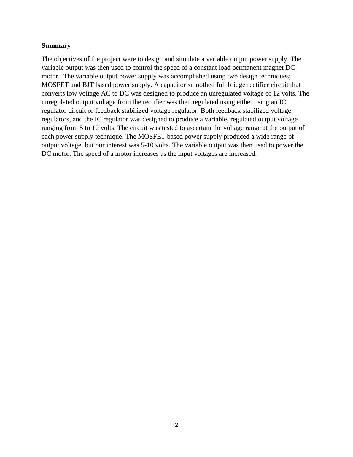
Figure 1.1 below shows feedback stabilized voltage regulator. The voltage regulator uses a
principle of negative feedback to keep the voltage at its output constant despite the variation in
its input.. Transistor Q1 acts as a control element, resistor R4, and Zener diode forms the
reference element. The voltage divider is comprising of resistors R1 and R2. The voltage divider
feeds back the output voltage to the base of transistor Q2. This feedback voltage controls the
flow of current in the collector keeping the voltage constant[1].
Figure 1.1: feedback stabilized voltage regulator. Source [1]
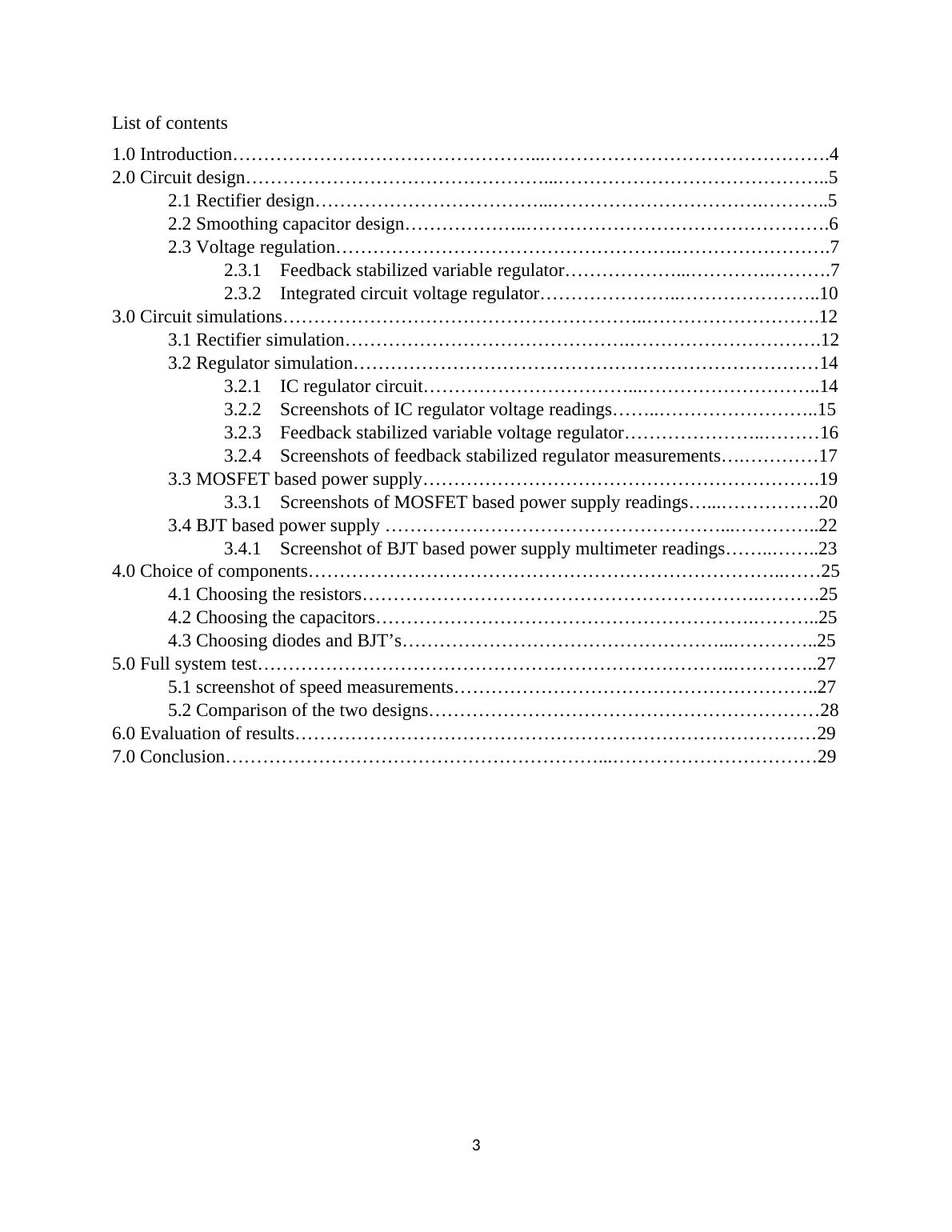
The adjustable voltage regulator can be achieved by using an integrated circuit regulator. The
integrated circuit regulator has three terminals, input and output voltage, and adjustable
terminals. Figure 1.2 shows an IC voltage regulator. The output voltage can be adjusted using
equation 1.1
Vout = Vref * (1 + R 2
R 1 )..............................................1.1
4
The project aims to design a variable voltage direct current power supply that will be used to
vary the speed of a motor. Two design approaches are used to achieve variable power supply;
BJT and MOSFET based power supply. BJT based power supply is formed by connecting a full-
wave bridge rectifier smoothen by a capacitor to feedback stabilized voltage regulator. MOSFET
based power supply is formed by connecting a rectifier with an IC regulator circuit.
Personal safety, injury and accident prevention, and compliance with environmental and health
laws and regulations are key to success in every project. It is a student’s responsibility to keep
themselves informed of the conditions affecting their safety and health. It is also their
responsibility to adhere to health and safety practices in the classroom and the laboratory. Each
individual in a working area is expected to perform all work safely to promote good health and
safety practices. Other practices that promote a safe workplace are hazard identification and
correction, the shutdown of dangerous activities, and proper plans of emergency response.
Figure 1.1 below shows feedback stabilized voltage regulator. The voltage regulator uses a
principle of negative feedback to keep the voltage at its output constant despite the variation in
its input.. Transistor Q1 acts as a control element, resistor R4, and Zener diode forms the
reference element. The voltage divider is comprising of resistors R1 and R2. The voltage divider
feeds back the output voltage to the base of transistor Q2. This feedback voltage controls the
flow of current in the collector keeping the voltage constant[1].
Figure 1.1: feedback stabilized voltage regulator. Source [1]
The adjustable voltage regulator can be achieved by using an integrated circuit regulator. The
integrated circuit regulator has three terminals, input and output voltage, and adjustable
terminals. Figure 1.2 shows an IC voltage regulator. The output voltage can be adjusted using
equation 1.1
Vout = Vref * (1 + R 2
R 1 )..............................................1.1
4
The LM317H develops a 1.25V voltage reference between its output and adjustment terminal.
Placing resistor R1 between the output and adjustment terminal causes a constant current to flow
through resistor R1 and down to the ground through R2 to set the overall output voltage [2].
Figure 1.2 IC voltage regulator
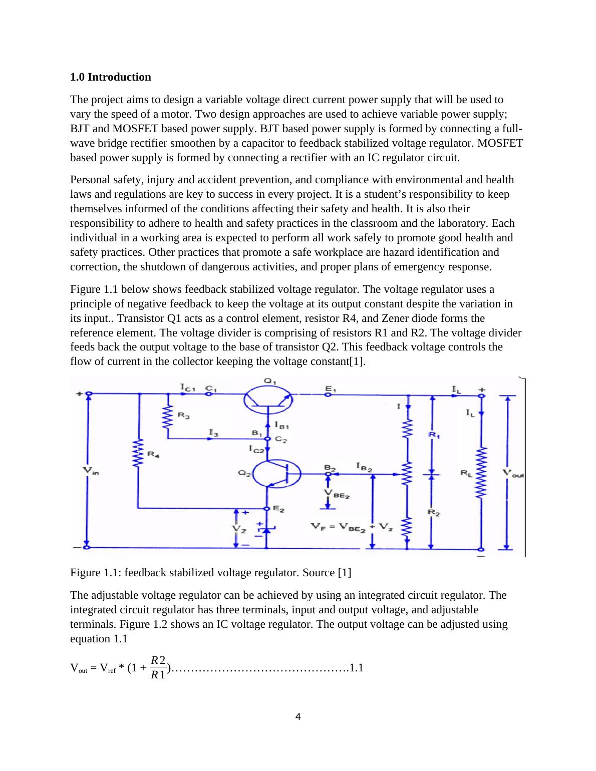
2.0 Circuit design
The power supply circuit consists of four main parts: a transformer, rectifier, a smoothing
capacitor, and a series regulator. The figure 2.1 shows parts of a DC power supply
Figure 2.1 power supply circuit. Source: [2]
The transformer converts 230V AC from the mains to an alternating current of about 12V,
depending on its ratings. The rectifier circuit employs four diodes, to transform the alternating
current to direct current. Smoothing capacitor reduces the quantity of alternating current ripple
on direct current voltage[3]. The regulator can either be BJT or MOSFET based; the two
techniques will be analyzed in detail.
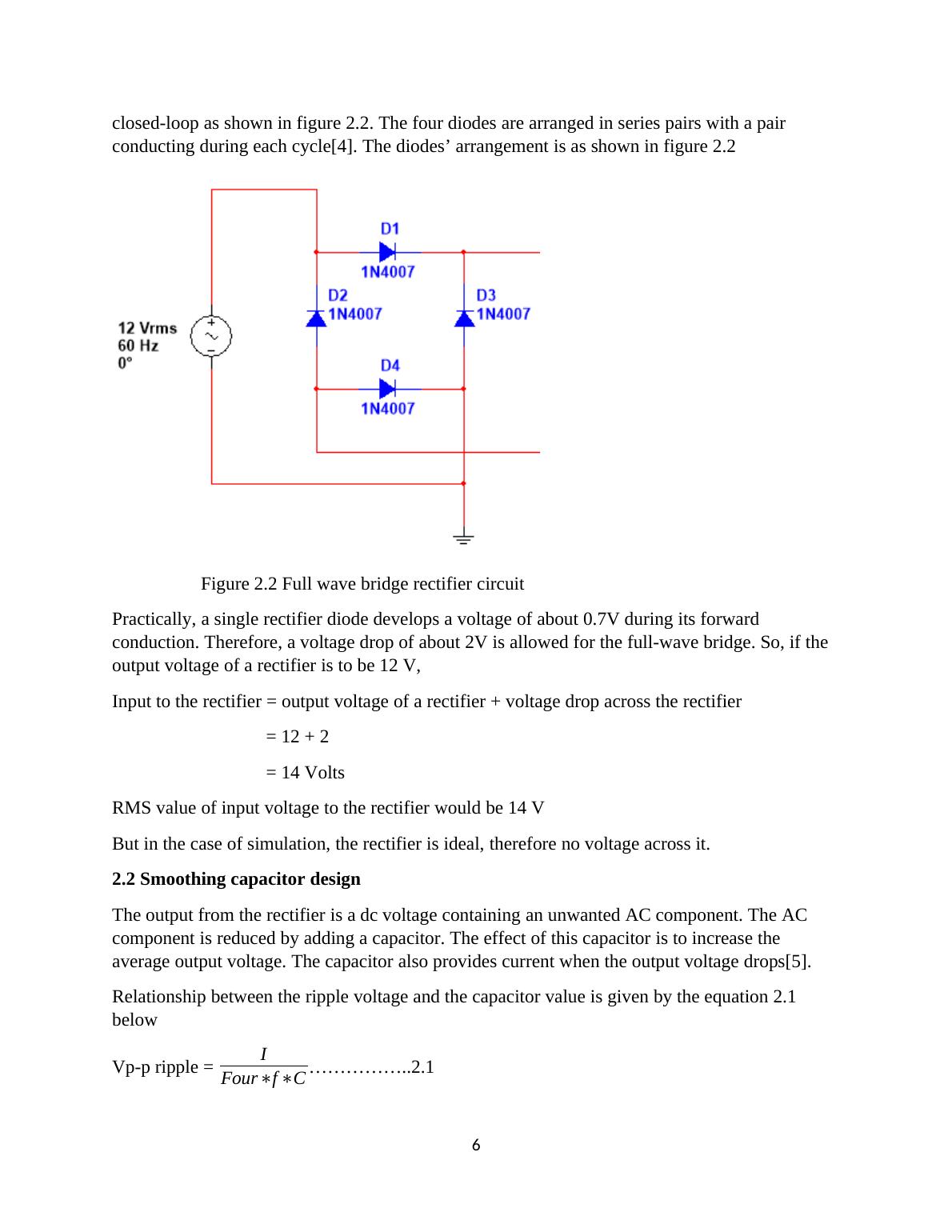
2.1 Rectifier design
Rectification of alternating current is achieved using a full-wave rectifier. A full-wave rectifier
accepts single phase input voltage. The bridge is using four diodes connected together in a
5
Placing resistor R1 between the output and adjustment terminal causes a constant current to flow
through resistor R1 and down to the ground through R2 to set the overall output voltage [2].
Figure 1.2 IC voltage regulator
2.0 Circuit design
The power supply circuit consists of four main parts: a transformer, rectifier, a smoothing
capacitor, and a series regulator. The figure 2.1 shows parts of a DC power supply
Figure 2.1 power supply circuit. Source: [2]
The transformer converts 230V AC from the mains to an alternating current of about 12V,
depending on its ratings. The rectifier circuit employs four diodes, to transform the alternating
current to direct current. Smoothing capacitor reduces the quantity of alternating current ripple
on direct current voltage[3]. The regulator can either be BJT or MOSFET based; the two
techniques will be analyzed in detail.
2.1 Rectifier design
Rectification of alternating current is achieved using a full-wave rectifier. A full-wave rectifier
accepts single phase input voltage. The bridge is using four diodes connected together in a
5
closed-loop as shown in figure 2.2. The four diodes are arranged in series pairs with a pair
conducting during each cycle[4]. The diodes’ arrangement is as shown in figure 2.2
Figure 2.2 Full wave bridge rectifier circuit
Practically, a single rectifier diode develops a voltage of about 0.7V during its forward
conduction. Therefore, a voltage drop of about 2V is allowed for the full-wave bridge. So, if the
output voltage of a rectifier is to be 12 V,
Input to the rectifier = output voltage of a rectifier + voltage drop across the rectifier
= 12 + 2
= 14 Volts
RMS value of input voltage to the rectifier would be 14 V
But in the case of simulation, the rectifier is ideal, therefore no voltage across it.
2.2 Smoothing capacitor design
The output from the rectifier is a dc voltage containing an unwanted AC component. The AC
component is reduced by adding a capacitor. The effect of this capacitor is to increase the
average output voltage. The capacitor also provides current when the output voltage drops[5].
Relationship between the ripple voltage and the capacitor value is given by the equation 2.1
below
Vp-p ripple = I
Four∗f ∗C .................2.1
6
End of preview
Want to access all the pages? Upload your documents or become a member.
Related Documents
The Buck Converterlg...
|5
|931
|58
Switch Mode Power Supply and its Typeslg...
|9
|1316
|416
Electromagnetic Compatibility Engineeringlg...
|14
|1135
|17
Design and Develop of Power Factor Correction Assignmentlg...
|12
|1627
|83
Speed Control of D.C Motorlg...
|15
|2246
|372
Speed Control Techniques in Brushless DC Motors Report 2022lg...
|8
|1344
|16