Design Analysis: Three Concentric Half Ring Microstrip Antenna
VerifiedAdded on 2023/04/19
|9
|1748
|99
Project
AI Summary
This project report details the design and analysis of a three concentric half ring microstrip patch antenna, undertaken at BHEL Electronics. The project aimed to design an efficient antenna suitable for military devices, wireless fidelity, and WLAN applications. The design process involved using HFSS electromagnetic simulation software, testing with a network analyzer, and comparing experimental results with desired outcomes. The report covers the project's background, objectives, the author's role as Chief Electronics Engineer, and responsibilities throughout the project. It also discusses the theoretical underpinnings, engineering knowledge applied, accomplishments, identified issues (such as VNA usage and HFSS simulation challenges), and solutions implemented. The project concluded with a proposed design that achieved high gain and minimum return loss, validated through simulation and testing.
CE 2.1 Project Information
Name of the project: Design and Analysis of Three Concentric Half Ring Microstrip
Patch Antenna
Location of the project: Bengaluru, Karnataka, India
Project Duration: Please fill
Organization: BHEL Electronics, India
Role and Designation during the time: Team Member of the project and Chief
Electronics Engineer
CE 2.2 Project Background
CE 2.2.1 Characteristics of the project
While working in BHEL Electronics organization, I got the idea of executing a project
on three concentric half ring microstrip patch antenna. The communication devices are
considered as one of the major and the most significant requirements for every individual for
communicating with other individuals. Electromagnetic waves are transmitted into the space
after converting electric power to radio waves. Various types of antennas are present,
however, I have selected microstrip antenna in this particular project. Various advantages like
easy plantation and easy designing were the major reasons that I selected microstrip antenna.
I designed and analyzed a three concentric half ring microstrip antenna. The proposed
antenna was being fed with a coaxial feed which is a contacting feed and was easy to
fabricate. Therefore, in this project, I provided a design for the microstrip antenna for making
it more improvised and effective.
Paraphrase This Document
Need a fresh take? Get an instant paraphrase of this document with our AI Paraphraser
CE 2.2.2 Objectives developed for the project
I had to ensure that my proposed design is perfect and is quite efficient and effective.
I designed a 3 concentric half ring microstrip antenna so that the half rings are arranged in a
cascaded fashion to increase the gain parameter. Hence, to complete the project with utmost
efficiency as well as priority, some of the important objectives were developed by me.
To design as well as analyze a three concentric half ring microstrip antenna.
To increase the gain parameter and reduce return loss of the microstrip antenna for
maintaining efficiency.
To make the antenna applicable for military devices, wireless fidelity and also
applications of WLAN.
To complete the entire simulation of the project with the help of High Frequency
Structural Simulator or HFSS electromagnetic simulation software tool.
To test the simulation results with the help of a network analyzer.
To set up the entire experiment with proper tools and techniques.
To match and contrast the experimental result with my desired results.
CE 2.2.3 My area of work
Being a successful electronics engineer, it was quite easier for me to provide the
design of the three concentric half ring microstrip patch antenna and hence I was selected as
the chief electronics engineer. I had been experimenting with various types of antenna for
several days and thus, when I got the chance of executing such a project, I selected HFSS
electromagnetic simulation software tool as the project integration software. My project
supervisor has confidence on me and gave the core responsibility of designing the project.
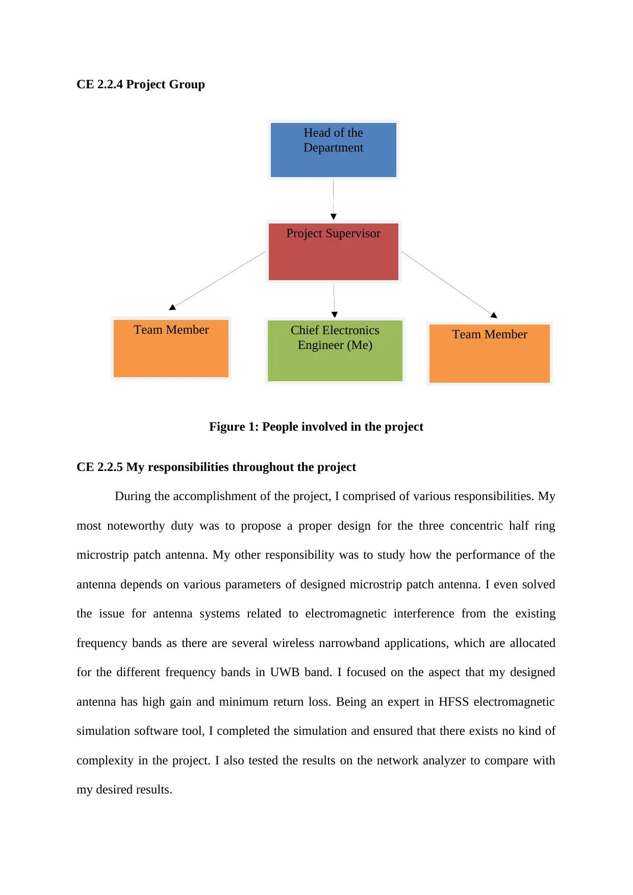
Head of the
Department
Project Supervisor
Chief Electronics
Engineer (Me)
Team Member Team Member
CE 2.2.4 Project Group
Figure 1: People involved in the project
CE 2.2.5 My responsibilities throughout the project
During the accomplishment of the project, I comprised of various responsibilities. My
most noteworthy duty was to propose a proper design for the three concentric half ring
microstrip patch antenna. My other responsibility was to study how the performance of the
antenna depends on various parameters of designed microstrip patch antenna. I even solved
the issue for antenna systems related to electromagnetic interference from the existing
frequency bands as there are several wireless narrowband applications, which are allocated
for the different frequency bands in UWB band. I focused on the aspect that my designed
antenna has high gain and minimum return loss. Being an expert in HFSS electromagnetic
simulation software tool, I completed the simulation and ensured that there exists no kind of
complexity in the project. I also tested the results on the network analyzer to compare with
my desired results.
⊘ This is a preview!⊘
Do you want full access?
Subscribe today to unlock all pages.

Trusted by 1+ million students worldwide
CE 2.3 Distinctive Activity
CE 2.3.1 Comprehending the Theory of Project
This project is a simulation based study of new proposed microstrip patch antenna
which has high gain and minimum return loss which makes antenna efficient to radiate. I
designed and verified a new conventional half ring microstrip patch antenna practically. I
arranged the half rings in a cascaded fashion for increasing the gain parameter. The narrow
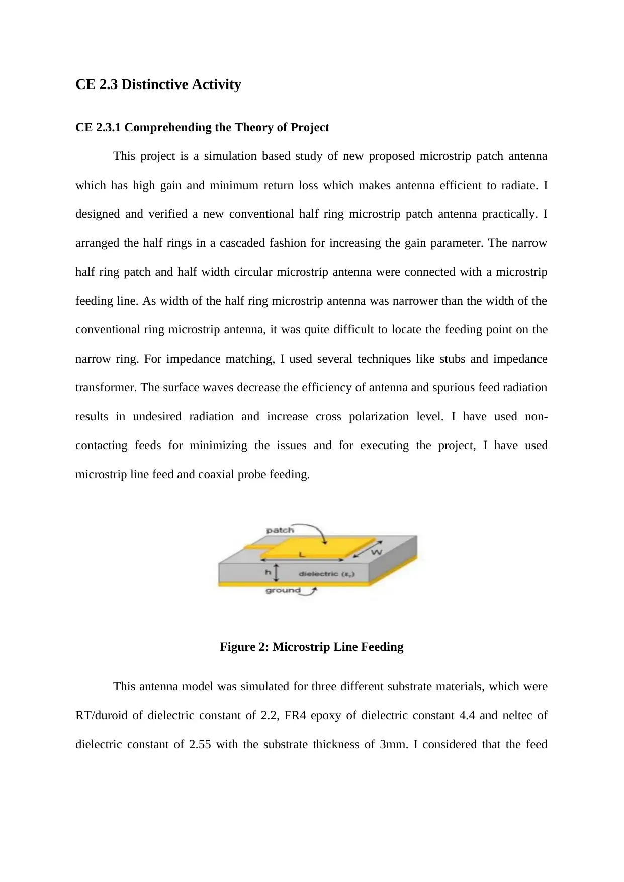
half ring patch and half width circular microstrip antenna were connected with a microstrip
feeding line. As width of the half ring microstrip antenna was narrower than the width of the
conventional ring microstrip antenna, it was quite difficult to locate the feeding point on the
narrow ring. For impedance matching, I used several techniques like stubs and impedance
transformer. The surface waves decrease the efficiency of antenna and spurious feed radiation
results in undesired radiation and increase cross polarization level. I have used non-
contacting feeds for minimizing the issues and for executing the project, I have used
microstrip line feed and coaxial probe feeding.
Figure 2: Microstrip Line Feeding
This antenna model was simulated for three different substrate materials, which were
RT/duroid of dielectric constant of 2.2, FR4 epoxy of dielectric constant 4.4 and neltec of
dielectric constant of 2.55 with the substrate thickness of 3mm. I considered that the feed
Paraphrase This Document
Need a fresh take? Get an instant paraphrase of this document with our AI Paraphraser
position was being placed, in which the input impedance was low and at a distance of 6.9mm
at the angle of 450 from center of circular patch.
CE 2.3.2 Engineering knowledge and skills applied in the project
To execute the project, I had applied my understanding of digital system designing,
antenna wave propagation and communication system for this project. For making the
microstrip patch antenna efficient, I have utilized several techniques and technologies of
electronics engineering. With core understanding in antenna and circuit designing, it was
quite easier for me to complete the project with higher efficiency. I have also applied my
knowledge of High Frequency Structural Simulator to complete the software integration
effectively.
CE 2.3.3 Accomplishment and Task Performed
In the beginning of the project, I at first considered single concentric and two
concentric half ring microstrip patch antennas. I got subsequent results from the experiments
and observed that the return loss obtained were not optimum. The one ring antenna provided
extremely higher return loss, which was not considerable. Regarding two ring microstrip
patch antenna, I noted that the return loss was better than one ring; however was not
appropriate in terms of my desired results. Therefore, I selected three concentric half ring
microstrip patch antenna for obtaining desired gain and return loss. I chose feed location in
patch boundaries, in which the input impedance matching was done, i.e. 50Ω.
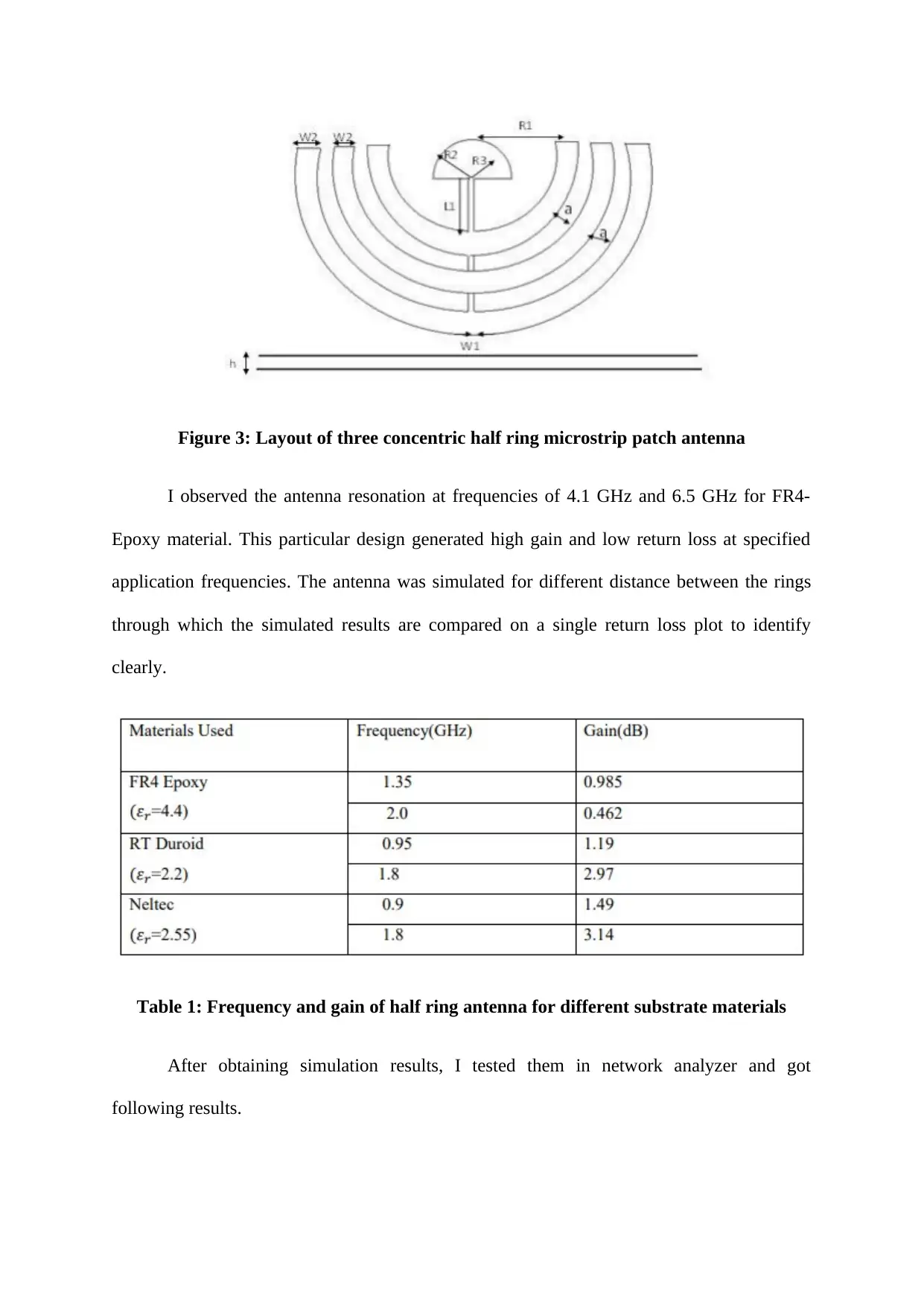
Figure 3: Layout of three concentric half ring microstrip patch antenna
I observed the antenna resonation at frequencies of 4.1 GHz and 6.5 GHz for FR4-
Epoxy material. This particular design generated high gain and low return loss at specified
application frequencies. The antenna was simulated for different distance between the rings
through which the simulated results are compared on a single return loss plot to identify
clearly.
Table 1: Frequency and gain of half ring antenna for different substrate materials
After obtaining simulation results, I tested them in network analyzer and got
following results.
⊘ This is a preview!⊘
Do you want full access?
Subscribe today to unlock all pages.

Trusted by 1+ million students worldwide
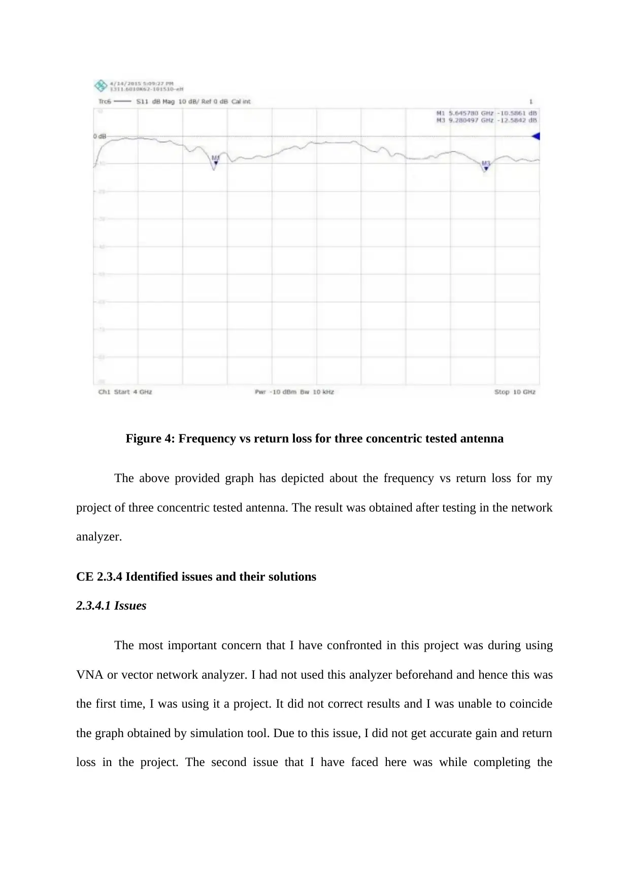
Figure 4: Frequency vs return loss for three concentric tested antenna
The above provided graph has depicted about the frequency vs return loss for my
project of three concentric tested antenna. The result was obtained after testing in the network
analyzer.
CE 2.3.4 Identified issues and their solutions
2.3.4.1 Issues
The most important concern that I have confronted in this project was during using
VNA or vector network analyzer. I had not used this analyzer beforehand and hence this was
the first time, I was using it a project. It did not correct results and I was unable to coincide
the graph obtained by simulation tool. Due to this issue, I did not get accurate gain and return
loss in the project. The second issue that I have faced here was while completing the
Paraphrase This Document
Need a fresh take? Get an instant paraphrase of this document with our AI Paraphraser
simulation with HFSS software. I faced major trouble while simulating this project and this
delayed my project.
2.3.4.2 Solutions
For the first problem of VNA, I attended workshops and took help from my
supervisor. Finally, I was able to obtain and plot the graph using VNA and was also able to
coincide with the graph obtained in the simulation tool. I noted that the antenna radiated at
frequency 5.6GHz and 9.4GHz. Regarding the second issue, I tried several times and finally
was able to obtain the results properly.
CE 2.3.5 Plan to produce creative and innovative work
For completing this project of the Design and Analysis of Three Concentric Half Ring
Microstrip Patch Antenna, I have to create the distinctive plan to produce outstanding design.
Being one of the electronics engineer, I had to make the design for this particular project.
CE 2.3.6 Collaborative Work
I had provided suggestions to my team to work altogether for becoming stress free for
each one of us for making this project effective. I also distributed different tasks equally
amongst my team members and then undertook regular work follow-ups.
CE 2.4 Project Review
CE 2.4.1 Project Overview
The key purpose of this project was proposing a suitable design for half ring
microstrip antenna. For this particular purpose, I had to use my information of antennas and
HFSS software to integrate the design. With proper testing and simulation in network
analyzer and HFSS software, I was able to execute the project effectively.

CE 2.4.2 My Contribution to work
I was assigned as the chief electronics engineer in this detailed project of Design and
Analysis of Three Concentric Half- Ring Microstrip Patch Antenna. My chief contribution
was proposing the accurate design for this project and also solving the several issues faced by
us.
I was assigned as the chief electronics engineer in this detailed project of Design and
Analysis of Three Concentric Half- Ring Microstrip Patch Antenna. My chief contribution
was proposing the accurate design for this project and also solving the several issues faced by
us.
⊘ This is a preview!⊘
Do you want full access?
Subscribe today to unlock all pages.

Trusted by 1+ million students worldwide
1 out of 9
Related Documents
Your All-in-One AI-Powered Toolkit for Academic Success.
+13062052269
info@desklib.com
Available 24*7 on WhatsApp / Email
![[object Object]](/_next/static/media/star-bottom.7253800d.svg)
Unlock your academic potential
Copyright © 2020–2026 A2Z Services. All Rights Reserved. Developed and managed by ZUCOL.


