Implementation of FPGA Technology for Digital Modem
VerifiedAdded on 2023/01/18
|11
|3194
|93
AI Summary
This report focuses on the implementation of FPGA technology for designing and implementing a digital modem. It includes a literature review, design methodologies, and project timeline.
Contribute Materials
Your contribution can guide someone’s learning journey. Share your
documents today.

FPGA Implementation of digital
modem
modem
Secure Best Marks with AI Grader
Need help grading? Try our AI Grader for instant feedback on your assignments.
FPGA
1
Abstract
FPGA is defined as the field programmable gate array which is an integrated circuit that
can be programmed in the field after manufacture. Mainly, such kind of technology is
used in the design and implementation of particularly integrated circuits which can
later be produced hard wired in huge quantities [8]. It is observed that the FPGA
technology allow consumers to tailor microprocessors in order to meet their
requirements. This report is completely based on the GPGA technology along with their
implementation process. A literature review will be conducted in this research study in
order to analyse the viewpoints of other experts and researchers about FPGA
technology. This report is divided into several sections, for example, statement of
design, literature review, design methodologies, project timeline.
FPGA
2
Aims and objectives
There are numerous aims and objectives of this study which are described below:
To analyse the concept of FPGA technology
To evaluate and implement the GPGA technology for digital modern
To enhance skills and experience in the field of FPGA
For achieving all the above aims and objectives a literature review and design
methodology sections will be involved where the researchers will provide in-depth
analyse about FPGA implementation. In the literature review section, there are numbers
of research papers will be discussed along with the research gaps and collect opinions
of other researchers on the implementation of FPGA.
Statement of design
For designing and implementing the digital modem on FPGA technology the frequency
modulation and demodulation processes can be used because it is one of the effective
techniques for modulating the applied frequency signals. The FM modulator will modify
the frequency of the applied signal by multiplying with the carrier signals and the
receiver will receive the effective output by using this technique [9]. The simulation
process will be done with the help of FPGA technology and Xilinx ISE software will be
adopted for synthesis and implementation of the circuit.
This research proposal is completely based on the FPGA technology and
implementation of FM modem with the help of FPGA technique. Moreover, this paper
focuses on the fundamental concept of FM modem along with the FPGA process for
designing and implementing the frequency modulators.
The frequency modulation and demodulation is mainly used for supporting the DAB-T
and PMR standards but such kind of process can be used in the field of the digital
modem for improving the frequency level of applied input signals. The digital modem is
defined as the technique which adapts digital signals from one transmission networks
to another and this report will design and implement FPGA system of a digital modem
[9]. With the help of this research study, the students can enhance their skills and they
can easily understand the fundamental working of FPGA technology with the digital
FPGA
3
modem. In this study, an FPGA implementation of a digital modem will be done for
targeting the software defined radio (SDR) applications. Both modulator and
demodulator involve a compressed direct digital synthesizer (DDS) for producing the
carrier frequency waves in order to modulate the input signal.
The demodulation process will be done with the help of a digital phase locked loop
(DPLL) approach because it is one of the best processes for collecting the information
and signals from modulated signals. However, the proposed digital modem will be
implemented with the help of Virtex 2 pro device and FPGA chip will be used for
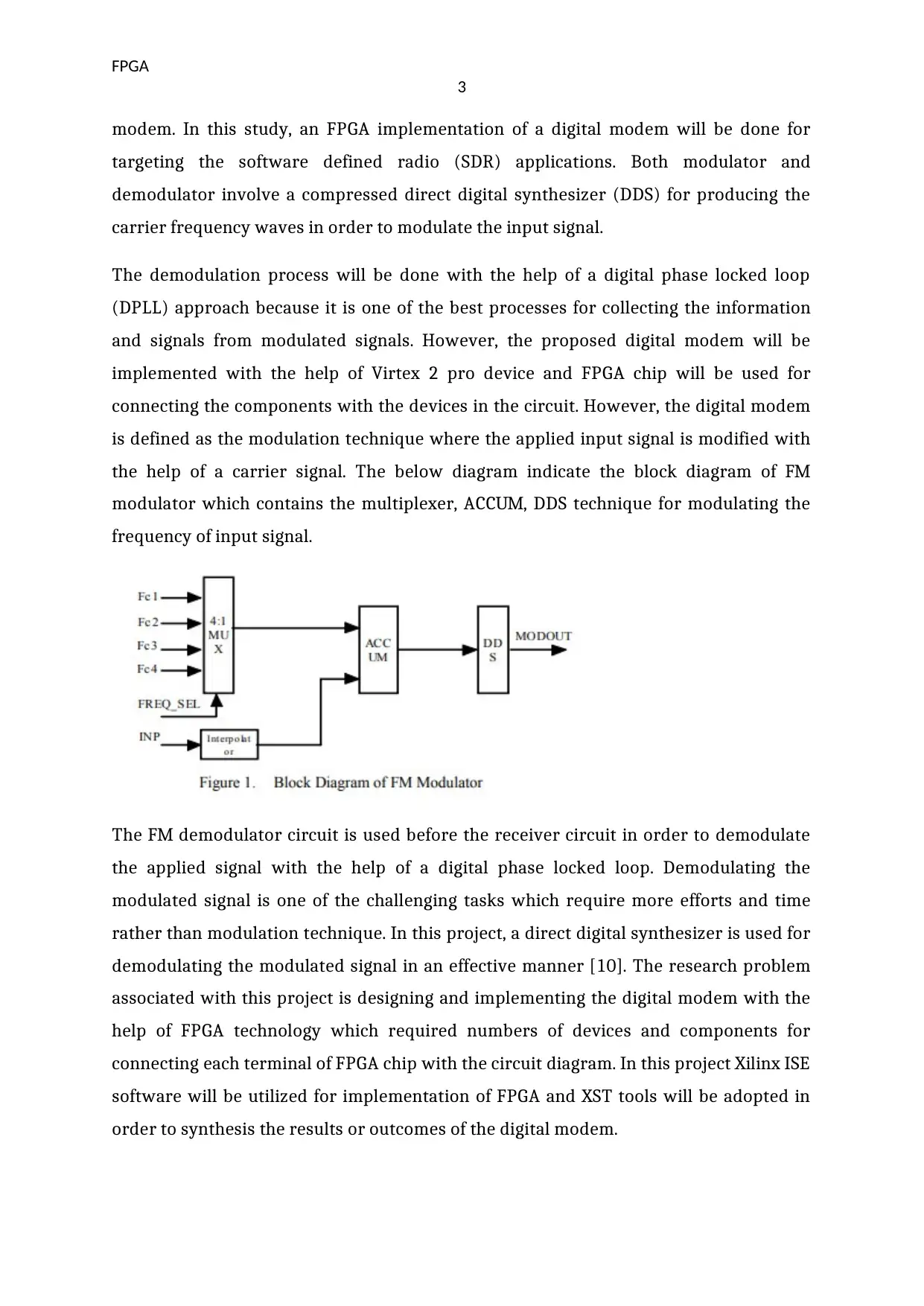
connecting the components with the devices in the circuit. However, the digital modem
is defined as the modulation technique where the applied input signal is modified with
the help of a carrier signal. The below diagram indicate the block diagram of FM
modulator which contains the multiplexer, ACCUM, DDS technique for modulating the
frequency of input signal.
The FM demodulator circuit is used before the receiver circuit in order to demodulate
the applied signal with the help of a digital phase locked loop. Demodulating the
modulated signal is one of the challenging tasks which require more efforts and time
rather than modulation technique. In this project, a direct digital synthesizer is used for
demodulating the modulated signal in an effective manner [10]. The research problem
associated with this project is designing and implementing the digital modem with the
help of FPGA technology which required numbers of devices and components for
connecting each terminal of FPGA chip with the circuit diagram. In this project Xilinx ISE
software will be utilized for implementation of FPGA and XST tools will be adopted in
order to synthesis the results or outcomes of the digital modem.
3
modem. In this study, an FPGA implementation of a digital modem will be done for
targeting the software defined radio (SDR) applications. Both modulator and
demodulator involve a compressed direct digital synthesizer (DDS) for producing the
carrier frequency waves in order to modulate the input signal.
The demodulation process will be done with the help of a digital phase locked loop
(DPLL) approach because it is one of the best processes for collecting the information
and signals from modulated signals. However, the proposed digital modem will be
implemented with the help of Virtex 2 pro device and FPGA chip will be used for
connecting the components with the devices in the circuit. However, the digital modem
is defined as the modulation technique where the applied input signal is modified with
the help of a carrier signal. The below diagram indicate the block diagram of FM
modulator which contains the multiplexer, ACCUM, DDS technique for modulating the
frequency of input signal.
The FM demodulator circuit is used before the receiver circuit in order to demodulate
the applied signal with the help of a digital phase locked loop. Demodulating the
modulated signal is one of the challenging tasks which require more efforts and time
rather than modulation technique. In this project, a direct digital synthesizer is used for
demodulating the modulated signal in an effective manner [10]. The research problem
associated with this project is designing and implementing the digital modem with the
help of FPGA technology which required numbers of devices and components for
connecting each terminal of FPGA chip with the circuit diagram. In this project Xilinx ISE
software will be utilized for implementation of FPGA and XST tools will be adopted in
order to synthesis the results or outcomes of the digital modem.
Secure Best Marks with AI Grader
Need help grading? Try our AI Grader for instant feedback on your assignments.
FPGA
4
Literature review
The FPGA implementation of the digital modem is one of the common topics for
research and in the last five years there are numbers of investigators provided their
views on this topic. The literature review section focuses on the design and
implementation of FPGA and analyses results obtained by previous journal papers. This
literature review will reduce the drawbacks and research gaps occurred in the previous
studies and help the students for analysing the fundamental concept of FPGA
implementation.
According to Ahmad and Gupta, (2013) the FPGA implementation can be performed
with the help of direct digital synthesizer and modulation techniques [1]. This journal
paper highlighted the concept of FPGA technology and implemented a digital FM
modem by using FPGA technique. The researchers analysed that both modulation and
demodulation process can be achieved with the help of the DDS technique and it allows
consumers to generate the carrier signals. After analysing this journal paper it has been
found that the implementations of frequency modulation modem can rum maximum
103 MHz frequency by taking around 8K gate equivalent in the FPGA device.
Atalik, et al., (2012) designed and implemented a digital modem by using modulation
and demodulation techniques [2]. After analysing this research paper it has been argued
that mixed demodulation is one of the best techniques for generating a digital FM
demodulator. The researchers implemented the digital FM modem on FPGA devices and
conducted a literature review in order to improve the effectiveness of the investigation.
The FM modulation is defined as the technique that has the potential to increase the
frequency of the input signal by multiplying with the carrier signal. From this paper, it is
analysed that the mixed demodulator technique takes less time for demodulating the
signal and information and the researchers used this approach for gathering the input
message.
Brito and Bampi, (2008) compared the results of FPGA implementation of FM
demodulator and other proposed systems [3]. The researchers also suggested that the
PLL is one of the effective demodulation techniques and it provides a way for
implementing the FM demodulation process with the help of FPGA technique. In this
research paper, a survey has been conducted by the authors for gathering viewpoints of
FPGA
5
other participants and observed that the PLL demodulator circuit can be implemented
by using a PLL process [11]. The authors involved a Modalism process for
implementation and simulation of FM modem and provided in-depth analysis of the
research topic.
According to Demirors, et al., (2015) the VCO is a very old technique which produces
numbers of challenges in the system due to which many consumers are using direct
digital synthesizer technique for modulating the applied signal [4]. In this paper,
numerous researches on the different architecture of FM demodulator have been
performed in order to realize an FM demodulator nitrated circuit. In this journal paper,
the researchers used FPGA Modelsim Xe 6.3c software in order to simulate and
implement the frequency modulation project on FPGA chip [16]. The researcher
identified that at the first phase of simulation, the demodulated output produces
overshoots since the phase synchronization is in convergence with the input phase and
after this stage, the overall system has been stabled.
Hatai and Chakrabarti, (2009) analysed that the synthesis optimization technique plays
a significant character in the field of FPGAs for achieving the large performance in terms
of resources utilization [5]. This paper identified the key aspects related to FPGA
technique and provided their opinions regarding synthesis optimization for finite
machine design. In order to analyse and implement the source code for FPGA, there are
various kinds of tools used, for example, Xilinx, Quartus, Altera and so on. Mainly, the
FPGA technique and software provide a platform for designing and implementing the
digital modem and variety of design constraints which can help the consumers to meet
the aims and objectives of projects [15]. This paper provided theoretical information
about FPGA technique and provided some information about synthesis optimization
technique which creates a research gap between the information and research question.
This literature review avoids all these research gaps and provides an in-depth analysis
of the research topic and involves the findings and results of previous research studies.
According to Jyothi, Jayaprakash and Gowda, (2015), the software defined ratio is
defined as a wireless communication system in which all of the signal processing is
implemented on FPGA technology [6]. This paper highlighted the applications of FPGA
technology and designed a digital FM demodulator system based on the 2nd order phase
locked loop. The researchers adopted an ADPLL technique for demodulating the
FPGA
6
modulated signals or messages because it is more effective and highly accurate which
reduce the distortions and provide an efficient signal to the receiver [12].
Kislal, Demiray, Ceylan and Yagci, (2015) identified that there are several other
technologies and methods by which the frequency of input signal can be computed from
the ratio of the in-phase and the quadrature components [7]. After evaluating this
research paper it has been found that digital implementation of FM demodulators in
software often does not meet the requirements of communication systems for which
many developers use FPGA technique. In the implementation of digital modem, there
are major two processes used such as FM modulation and FM demodulation process.
The modulation process helps the designers for improving the frequency of transferred
signals and demodulator process again demodulate the signal into original information.
Many researchers suggested that the DDS is the very best technique for implementing
digital modem where it improves the performance of the complete circuitry process
[13]. Therefore, it has been suggested that during generation and implementation of
digital modem the developers should adopt direct digital synthesize along with the PLL
demodulator process [14]. For implementing the coding and circuit diagram the Xilinx
software can be used that link the connecting wires with the electronic devices used in
the implementation of FPGA project.
Design methodology
Initially, the researchers can use modulation technique for modulating the input
message signals for which the FM modulator circuit can be adopted. Moreover, for
generating the carrier signals the direct digital synthesize technique can be used which
has the ability for improving the strength of the input signal. After that, an FM
demodulator circuit can be designed by using the concept of digital phase locked loop.
The demodulator circuit should involve several devices and techniques, for example,
modulation output, phase detector, loop filter, FIR filter, DDS and demodulation output.
For synthesize and implementation of results, Xilinx and FPGA software can be used
along with the Modalism Xe 6.3c tools for simulating the applied input signals. For
developing source code regarding the digital modem the MATLAB and FPGA tools can
be adopted. There are several methodologies and steps are used for completing this
project and achieving the effective results at the end of research which is the following:
Paraphrase This Document
Need a fresh take? Get an instant paraphrase of this document with our AI Paraphraser
FPGA
7
Training on software and FPGA tools
Research and study about the digital modem, modulation techniques and FPGA
technology
Design and simulate source code in FPGA software
Ordering devices and components used for implementing digital modem
Hands on with the development circuitry boards
Debugging
Testing and implementing digital modem on FPGA tools
Analysing results and findings
Final project submission
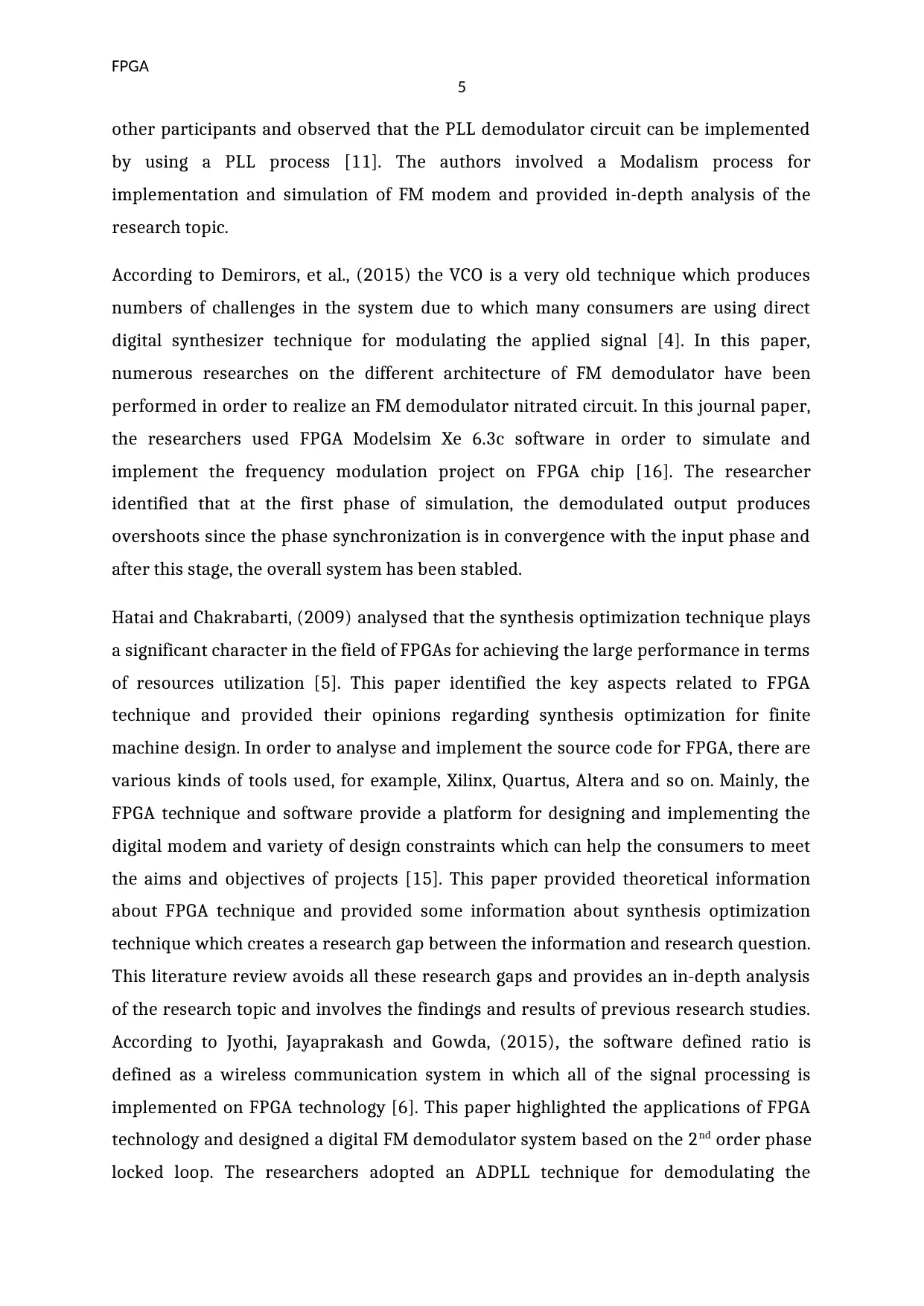
With the help of all these steps and methods, the digital modem project can be
implemented and simulate on the FPGA software. Therefore, the implementation of a
digital modem should be done in the assigned time by following all the above steps
along with the time plan.
Time plan
The time plan provides a brief idea about time duration required to complete this
research project and it can be done in the current semester. The time plan depends on
the various activities involved in the development and implementation of a digital
modem by using FPGA technology.
Finalise project
project proposal
training on coding
simulation process
order components and
devices
project report
6 60
30
25
30
10
Duration (Days)
Duration (Days)
7
Training on software and FPGA tools
Research and study about the digital modem, modulation techniques and FPGA
technology
Design and simulate source code in FPGA software
Ordering devices and components used for implementing digital modem
Hands on with the development circuitry boards
Debugging
Testing and implementing digital modem on FPGA tools
Analysing results and findings
Final project submission
With the help of all these steps and methods, the digital modem project can be
implemented and simulate on the FPGA software. Therefore, the implementation of a
digital modem should be done in the assigned time by following all the above steps
along with the time plan.
Time plan
The time plan provides a brief idea about time duration required to complete this
research project and it can be done in the current semester. The time plan depends on
the various activities involved in the development and implementation of a digital
modem by using FPGA technology.
Finalise project
project proposal
training on coding
simulation process
order components and
devices
project report
6 60
30
25
30
10
Duration (Days)
Duration (Days)
FPGA
8
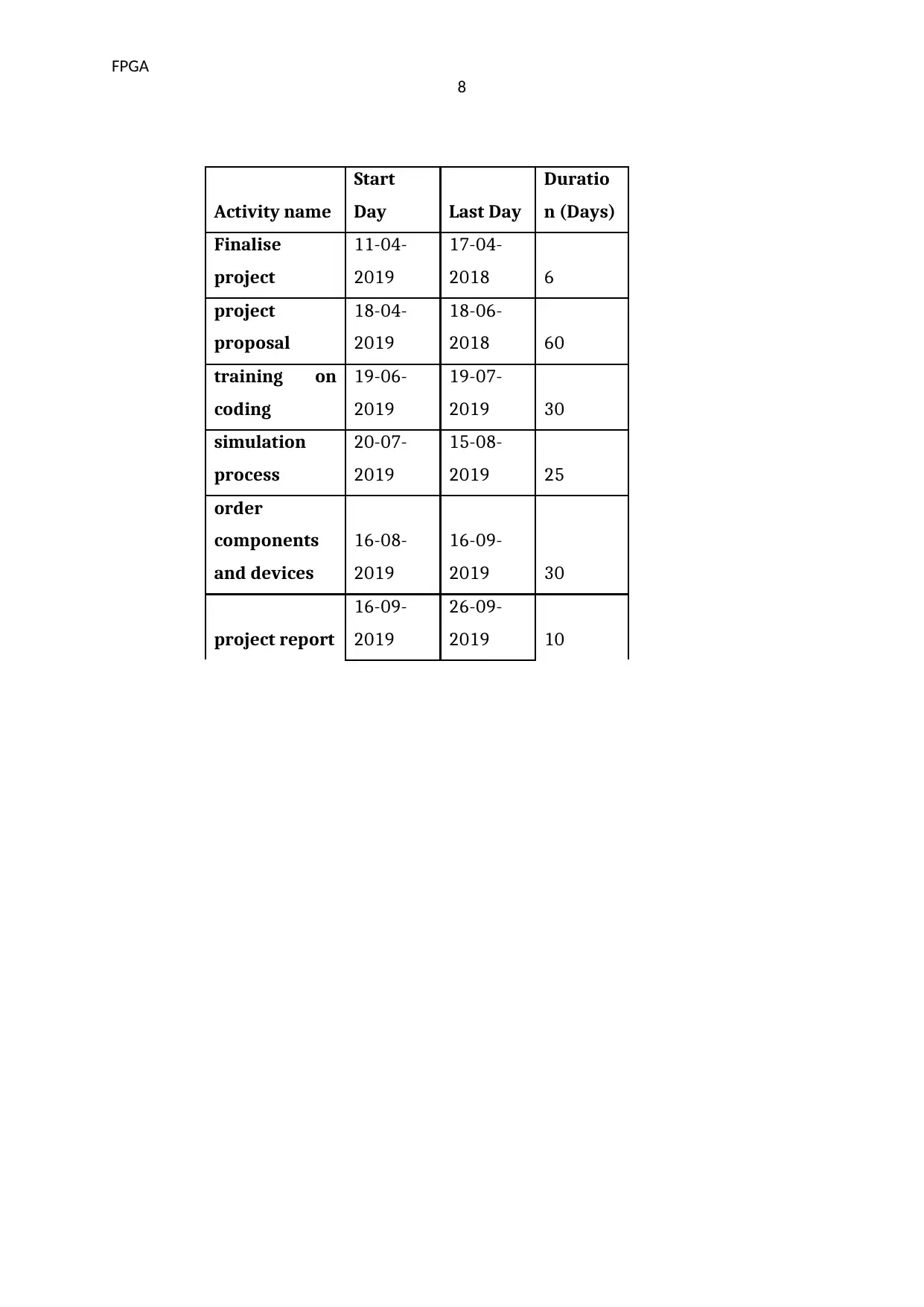
Activity name
Start
Day Last Day
Duratio
n (Days)
Finalise
project
11-04-
2019
17-04-
2018 6
project
proposal
18-04-
2019
18-06-
2018 60
training on
coding
19-06-
2019
19-07-
2019 30
simulation
process
20-07-
2019
15-08-
2019 25
order
components
and devices
16-08-
2019
16-09-
2019 30
project report
16-09-
2019
26-09-
2019 10
8
Activity name
Start
Day Last Day
Duratio
n (Days)
Finalise
project
11-04-
2019
17-04-
2018 6
project
proposal
18-04-
2019
18-06-
2018 60
training on
coding
19-06-
2019
19-07-
2019 30
simulation
process
20-07-
2019
15-08-
2019 25
order
components
and devices
16-08-
2019
16-09-
2019 30
project report
16-09-
2019
26-09-
2019 10
FPGA
9
References
[1]. A. Ahmad and, R., Gupta, “Digital PWM of cascaded multilevel voltage source
inverter using FPGA,” In 2013 Students Conference on Engineering and Systems
(SCES), vol. 12, no. 2, pp. 1-5, 2013.
[2]. T., Atalik, M., Deniz, E., Koc, C.Ö., Gercek, B., Gultekin, M. Ermis and I., Cadirci,
“Multi-DSP and-FPGA-based fully digital control system for cascaded multilevel
converters used in FACTS applications,” IEEE transactions on industrial
informatics, vol. 8, no. 3, pp.511-527, 2012.
[3]. J.P.M. Brito and S., Bampi, “Design of a digital FM demodulator based on a 2nd-
order all-digital phase-locked loop,” Analog Integrated Circuits and Signal
Processing, vol. 57, no. 1-2, pp.97-105, 2008.
[4]. E., Demirors, G., Sklivanitis, T., Melodia, S.N. Batalama and, D.A., Pados,
“Software-defined underwater acoustic networks: toward a high-rate real-time
reconfigurable modem,” IEEE Communications Magazine, vol. 53, no. 11, pp.64-
71, 2015.
[5]. I. Hatai and I., Chakrabarti, “FPGA implementation of a Digital FM Modem,”
In 2009 International Conference on Information and Multimedia Technology, vol.
12, no. 2, pp. 475-479, 2009.
[6]. N., Jyothi, S. Jayaprakash and, S.K., Gowda, “Design and VLSI implementation of
high performance DUC and DDC for software defined radio applications,” In 2013
International Conference on Emerging Trends in Communication, Control, Signal
Processing and Computing Applications (C2SPCA), vol. 4, no. 4, pp. 1-3, 2013.
[7]. A.O., Kislal, A., Demiray, O. Ceylan and, H.B., Yagci, “Implementation of software
defined FM mixed demodulator on FPGA,” In 2015 23rd Telecommunications
Forum Telfor (TELFOR), vol. 12, no. 1, pp. 333-336, 2015.
[8]. K.A., Kumar, “FPGA implementation of PSK modems using partial re-
configuration for SDR and CR applications,” In 2012 Annual IEEE India Conference
(INDICON), vol. 8, no. 5, pp. 205-209, 2012.
[9]. M. Kumar and, K., Lata, “FPGA implementation of ADPLL with Ripple Reduction
Techniques,” International Journal of VLSI Design and Communication Systems
(VLSICS), vol. 3, no. 2, pp.99-106, 2012.
Secure Best Marks with AI Grader
Need help grading? Try our AI Grader for instant feedback on your assignments.
FPGA
10
[10]. J. Mangala and, J., Manikandan, “FPGA implementation of reconfigurable
modulation system,” In 2015 International Conference on Advances in Computing,
Communications and Informatics (ICACCI), vol. 8, no. 2, pp. 493-500, 2015.
[11]. M.A., Mohamed, A.S. Samarah and, M.F., Allah, “Implementation of the
OFDM physical layer using FPGA,” International Journal of Computer Science
Issues (IJCSI), vol. 9, no. 2, p.612, 2012.
[12]. P. Noel and, M., Klemes, “Doubling the through-put of a digital microwave
radio system by the implementation of a cross-polarization interference
cancellation algorithm,” In 2012 IEEE Radio and Wireless Symposium, vol. 12, no.
8, pp. 363-366, 2012.
[13]. S.O., Popescu, A.S. Gontean and, G., Budura, “BPSK system on Spartan 3E
FPGA,” In 2012 IEEE 10th International Symposium on Applied Machine
Intelligence and Informatics (SAMI), vol. 8, no. 7, pp. 301-306, 2012.
[14]. M., Saber, Y. Jitsumatsu and, M.T.A., Khan, “Design and implementation of
low power digital phase-locked loop,” In 2010 International Symposium On
Information Theory & Its Applications, vol. 6, no. 7, pp. 928-933, 2010.
[15]. B.H., Tietche, O. Romain and, B., Denby, “A practical FPGA-based
architecture for arbitrary-ratio sample rate conversion,” Journal of Signal
Processing Systems, vol. 78, no. 2, pp.147-154, 2015.
[16]. R. Uma and, P., Dhavachelvan, “Synthesis Optimization For Finite State
Machine Design In Fpgas,” International Journal of VLSI Design & Communication
Systems, vol. 3, no. 6, p.79, 2012.
1 out of 11
Related Documents


Your All-in-One AI-Powered Toolkit for Academic Success.
+13062052269
info@desklib.com
Available 24*7 on WhatsApp / Email
![[object Object]](/_next/static/media/star-bottom.7253800d.svg)
Unlock your academic potential
© 2024 | Zucol Services PVT LTD | All rights reserved.