logo

Student. Professor. Principles and applications of Elec


Added on  2023-01-18

17 Pages1906 Words56 Views
Student
Professor
Principles and applications of Electronic Devices and Circuits
Date
Student. Professor. Principles and applications of Elec_1
1
TASK 1
A transistor amplifier circuit is used to amplify low voltage and current signals to higher
levels. The common-emitter configuration has higher efficiency in amplification of AC input
signals and is considered in many applications due to its characteristics:
I. High voltage gain
II. Moderate current gain
III. Medium input and output impedance
IV. Phase difference of input and output is 180 ° (Agarwal, 2019)
The transistor amplifier circuit to be built was assembled on Multisim as shown below:
Figure 1.1 Simulated circuit
Student. Professor. Principles and applications of Elec_2
2
The waveforms of the output and input were:
Figure 1.2 Waveforms
The first channel (top waveform) was connected to input while the output to channel
B(bottom waveform). From the amplitude difference of the input having 6.252mV and output
being 1.046V, the circuit amplified the input. It was also evident that phase difference of
input and output is 180 °
a) Values of R1 and R2 are altered
The bias circuit consists of a voltage divider bias with resistors R1 and R2. This scheme is
used due to its temperature resilience hence maintaining stability of the amplifier. (Sedra,
Smith and Chandorkar, 2009) The initial values for R1 with R2 were 4.7kΩ 1 kΩ respectively.
The resistor values used in investigating the effects of varying bias resistances were chosen
from the E24 resistor series.
Varying R1 with R2 constant yielded the following:
i. Reducing R1 to 3.3k
Student. Professor. Principles and applications of Elec_3
3
Figure 1.3
R1 is the forward bias base resistor. The output was clipped at the bottom after reducing R1
to 3.3k. It was also observed that the amplitude was greater than initial output. This is due
to the relation of R1 to the base voltage, V B.
From the voltage divider biasing:
V B =V CC
R2
R1+ R2
From the above equation and using DC analysis, a reduction in R1 causes a higher base
voltage, reducing the base drive current hence increasing the current at the collector. This is
reflected as greater amplification. However, the increase in base voltage causes a higher
emitter voltage since the forward bias voltage remains constant.
V E=V BV BE
V CE=V CV E
This causes a change in V CB making the transistor not operate at the quiescent point causing
the distortion of the output.
ii. Increasing R1 to 6.8k
Student. Professor. Principles and applications of Elec_4

End of preview

Want to access all the pages? Upload your documents or become a member.

Related Documents
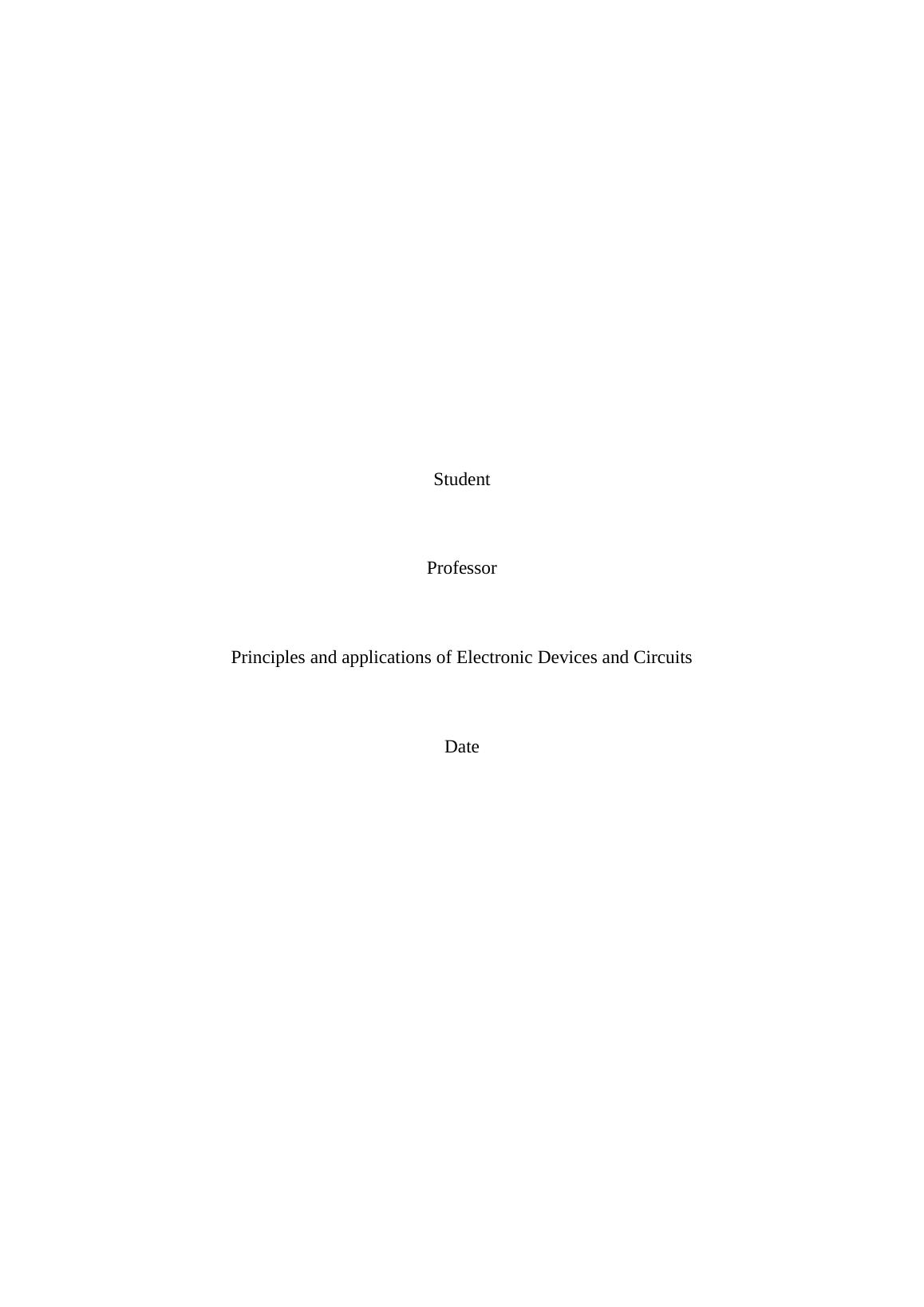
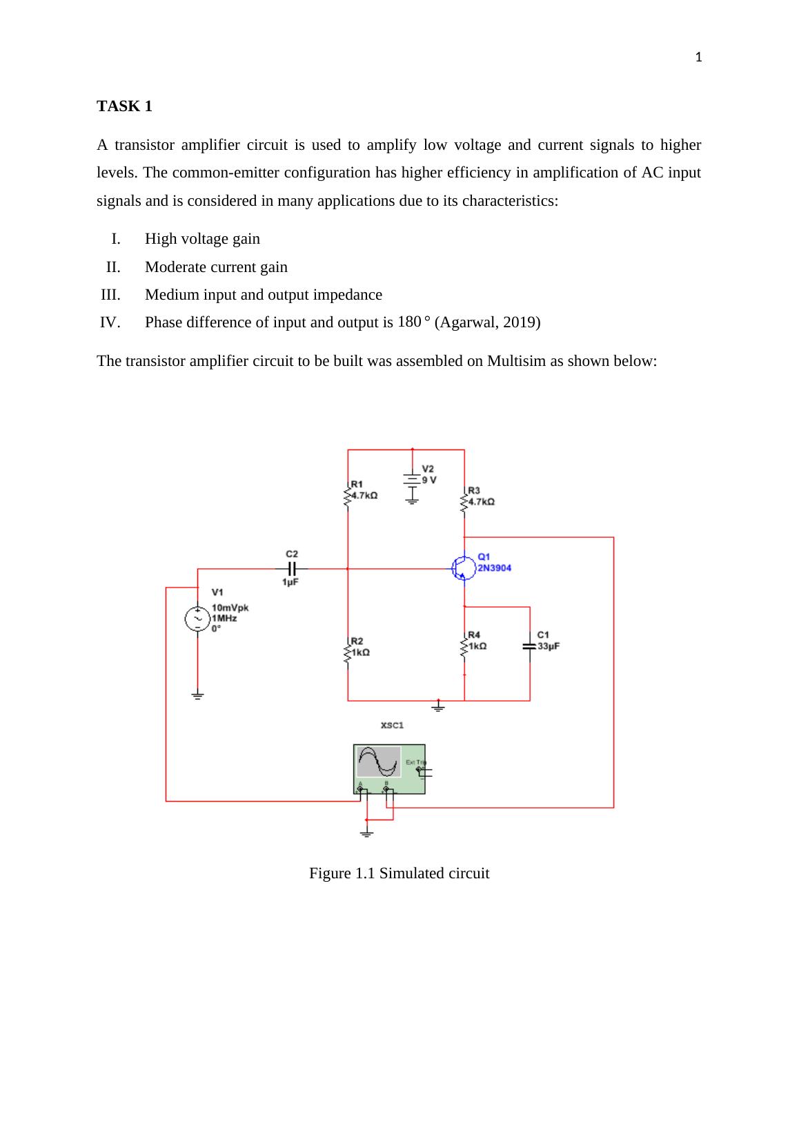
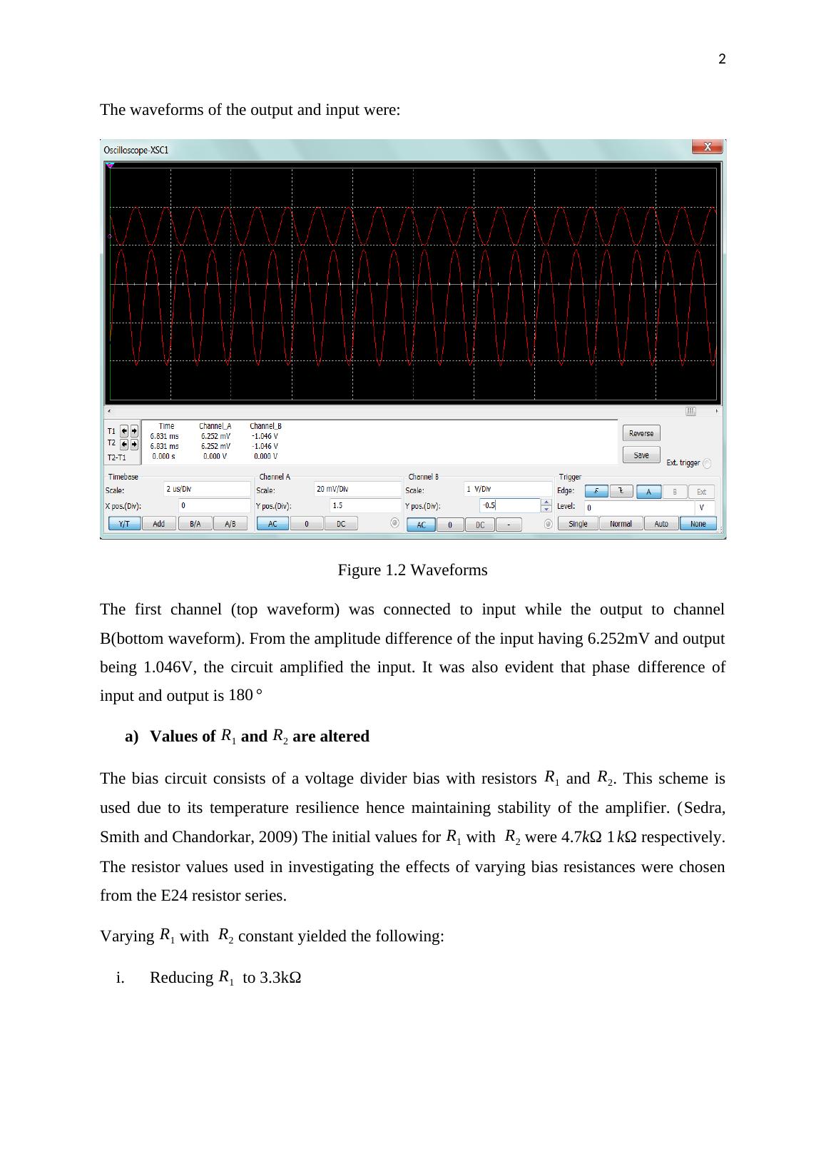
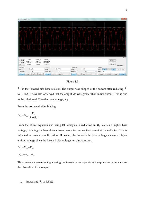
Principles and Applications of Electronic Devices and Circuits
|4
|1212
|69

Amplifiers: Types, Characteristics and Performance Tests
|31
|3026
|131

Evolution of Electronics and Solid State Control System
|10
|3707
|35

Power Amplifiers Design and Simulation | Report
|27
|3863
|37

Designing an Audio Amplifier: Steps and Analysis
|13
|2054
|268

Bipolar Transistor Amplifier- Abstract
|2
|552
|775