EN0720 Digital Electronic Design Automation Assignment
Added on 2020-05-04
55 Pages5319 Words80 Views
0VGDL
Table of ContentsTask – 1..................................................................................................................................................1Task - 2................................................................................................................................................12Task - 3................................................................................................................................................15Task - 4................................................................................................................................................19Task – 5................................................................................................................................................23Task - 6................................................................................................................................................26Task -7.................................................................................................................................................30Task -8.................................................................................................................................................34Task -9.................................................................................................................................................35Task -10...............................................................................................................................................38Task -11...............................................................................................................................................40Task -12...............................................................................................................................................42References...........................................................................................................................................46
Task – 1Create a System Verilog Source Descriptions for the ‘ManchTrans’ BlockThe timing diagram shows the behaviour of the signals associated with theManchester Encoding block. The non-return to zero data steam is considered as a pseudo-Random bit sequence. The PRBS contains the (2N-1) bits, where N is a parameter that sets thelength of the PRBS shift register. The main system of 100 MHz is divided as a result of databit rate which is10MBits/second. These pulses are achieved by means of an internal signal,where the pulses are high at one clock period, for every 10 bits/second. Figure 1: Internal diagram of Manchester transmitterThe above circuit diagram is the internal block diagram for the divider clock. It consists of I/O ports in the divider clock. This diagram explains the operation of the clock divider.Creating a SV Module for the Clock DividerThe parameters ‘DIVIDER’ and ‘N’ allow the division ratio. ‘N’ is the length of theregister to divide the ‘DIVIDER’. In the output, ‘bit_en’ from the ‘divclk’ module enables thepseudo-random bit sequence generator to shift out the next random data bit on the signal. Thedivider circuit system verilog module is created by using the vivado simulator. The dividerclock pulses include the bit encoder and bit clock. The below figure shows the system verilogmodule for the divider clock.1
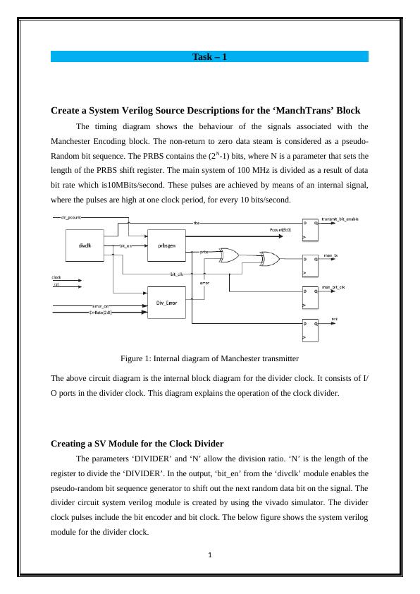
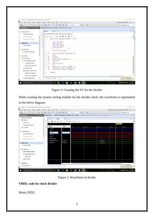
Figure 2: Creating the SV for the dividerWhile creating the system verilog module for the divider clock, the waveform is representedin the below diagram:Figure 3: Waveform of dividerVHDL code for clock dividerlibrary IEEE;2
use IEEE.STD_LOGIC_1164.ALL;useIEEE.numeric_std.ALL;entityClock_Divider isport ( clk,reset: in std_logic;clock_out: out std_logic);endClock_Divider;architecturebhv of Clock_Divider issignal count: integer:=1;signaltmp : std_logic := '0';beginprocess(clk,reset)beginif(reset='1') thencount<=1;tmp<='0';elsif(clk'event and clk='1') thencount<=count+1;if (count = 25000) thentmp<= NOT tmp;count<= 1;3
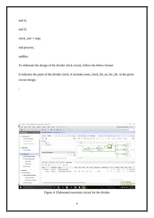
end if;end if;clock_out<= tmp;end process;endbhv;To elaborate the design of the divider clock circuit, follow the below format: It indicates the ports of the divider clock. It includes reset, clock, bit_en, bit_clk in the given circuit design.:Figure 4: Elaborated execution circuit for the divider4
Clock divider is also called as Frequency divider. This divider clock is used to dividethe frequency of the input clock and it also provides the output clock. Clock divider code ofthe VHDL consists of two inputs known as Clock and Reset input, and these input values aredivided using the divider clock. Thus, by this division the output clock is obtained. Thedivider clock has the clock source called CLK_PB4, if the process runs in a time then thereoccurs a change in the input clock value (The Muddy Engineer, 2017). The important factorthat is determined in the divider clock is the scaling factor. The formula for determining thescaling factor is represented below.Creating a SV Module for the Pseudo-Random Bit Sequence GeneratorThe pcount signal keeps track of the number of output bits, during each burst ofpseudo-random bits. Both ‘prbs’ and ‘pcount’ outputs are triggered by the input ‘bit_en’ andthe corresponding system clock edge. The ‘prbsgen’ module operates and verifies by thebehavioural simulation, with the help of the vivado simulator. Pseudo Random BinarySequence Generator (PRBS) is an important sequence of binary numbers which are arrangedrandomly. It is called as Pseudo if the value is deterministic and after certain number of nelements, it starts repeating. It is called as Random binary sequence, if the value of oneelement is independent with the other element. This generator is implemented by the use ofLinear Feedback Shift Register. This PRBS generator is used to produce the sequence ofbinary numbers (PRBS: Pseudo Random Binary Sequence, 2017). The following vhdl code isused to create the waveform, for the pseudo random binary sequence. Code for prbsgenlibrary IEEE;use IEEE.STD_LOGIC_1164.ALL;use IEEE.STD_LOGIC_ARITH.ALL;use IEEE.STD_LOGIC_UNSIGNED.ALL;5
entity prbsgen isport ( pclock : in STD_LOGIC;preset : IN std_logic := '0';prbsout : out STD_LOGIC);end prbsgen;architectureBehavioral of prbsgen isCOMPONENT dff isPORT(dclock : IN std_logic;dreset : IN std_logic;din : IN std_logic ;dout : OUT std_logic);END COMPONENT;signaldintern : std_logic_vector (4 downto 1);signal feedback : std_logic := '0';begininstdff :dff port map (pclock , preset , feedback , dintern(1));genreg : for i in 2 to 4 generatebegin6
End of preview
Want to access all the pages? Upload your documents or become a member.
Related Documents
Document on Assignment Circuitlg...
|15
|2132
|392
Assignment On State Machine Positive Edge Triggeredlg...
|2
|1003
|421