Evolution of Electronics and Solid State Control System
VerifiedAdded on 2023/01/17
|10
|3707
|35
AI Summary
This report explores the evolution of electronics and the rapid replacement of mechanical technology with solid state control systems. It discusses the design and testing of transistor amplifiers, oscillators based on Nor gates, and the 555 chip. The report also covers the design and testing of delay units and voltage controlled oscillators. It includes calculations for DC and AC voltage gains.
Contribute Materials
Your contribution can guide someone’s learning journey. Share your
documents today.
1
ABSTRACT.
Evolution of electronics has given birth to
mother of all inventions. Solid state
control system is rapidly replacing
outdated mechanical technology that has
been in use over decades. During olden
days, a simple task such as amplification
of small signals seemed like a mountain
task. All credit to the changing dynamics
of the solid state controls whereby such
task are easily implemented with easily
accessible devices such as transistors. In
this report, experiments have been carried
in the laboratory. The transistor amplifier,
oscillators based on Nor gate and the 555
chip have been physically built. In
addition, delay unit has been implemented.
The characteristics of theof various
components used have been investigated
under different circumstances and
condition. Analysis of the findings have
also been dealt with and conclusion made
on the same.
LITERATURE REVIEW.
Transistor amplifier.
Signal amplification is the process by
which amplifier circuit records amplified
output signal that is a version of the input
signal. The transistor amplifier as the name
denotes is the amplification circuitry that is
purely dependent on the transistor [1].
Common emitter Amplifier is the most
used configuration for transistors that are
based on NPN transistors. The transistor
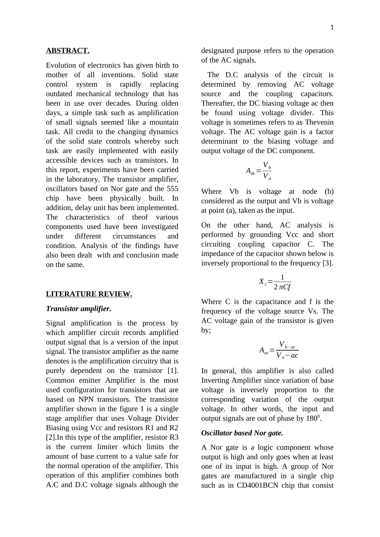
amplifier shown in the figure 1 is a single
stage amplifier that uses Voltage Divider
Biasing using Vcc and resistors R1 and R2
[2].In this type of the amplifier, resistor R3
is the current limiter which limits the
amount of base current to a value safe for
the normal operation of the amplifier. This
operation of this amplifier combines both
A.C and D.C voltage signals although the
designated purpose refers to the operation
of the AC signals.
The D.C analysis of the circuit is
determined by removing AC voltage
source and the coupling capacitors.
Thereafter, the DC biasing voltage ac then
be found using voltage divider. This
voltage is sometimes refers to as Thevenin
voltage. The AC voltage gain is a factor
determinant to the biasing voltage and
output voltage of the DC component.
Adc= V b
V a
Where Vb is voltage at node (b)
considered as the output and Vb is voltage
at point (a), taken as the input.
On the other hand, AC analysis is
performed by grounding Vcc and short
circuiting coupling capacitor C. The
impedance of the capacitor shown below is
inversely proportional to the frequency [3].
X c= 1
2 πCf
Where C is the capacitance and f is the
frequency of the voltage source Vs. The
AC voltage gain of the transistor is given
by;
Aac = V b−ac
V a−ac
In general, this amplifier is also called
Inverting Amplifier since variation of base
voltage is inversely proportion to the
corresponding variation of the output
voltage. In other words, the input and
output signals are out of phase by 1800.
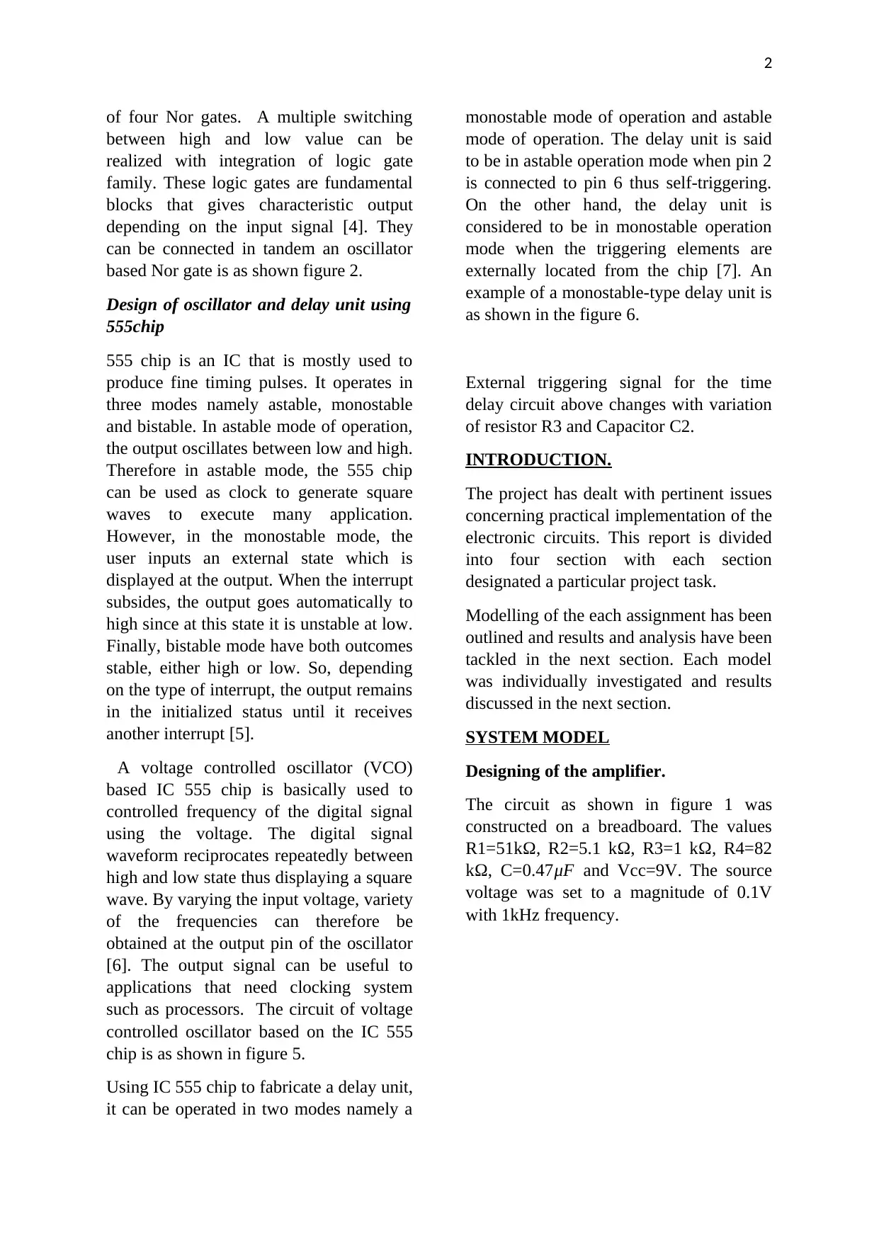
Oscillator based Nor gate.
A Nor gate is a logic component whose
output is high and only goes when at least
one of its input is high. A group of Nor
gates are manufactured in a single chip
such as in CD4001BCN chip that consist
ABSTRACT.
Evolution of electronics has given birth to
mother of all inventions. Solid state
control system is rapidly replacing
outdated mechanical technology that has
been in use over decades. During olden
days, a simple task such as amplification
of small signals seemed like a mountain
task. All credit to the changing dynamics
of the solid state controls whereby such
task are easily implemented with easily
accessible devices such as transistors. In
this report, experiments have been carried
in the laboratory. The transistor amplifier,
oscillators based on Nor gate and the 555
chip have been physically built. In
addition, delay unit has been implemented.
The characteristics of theof various
components used have been investigated
under different circumstances and
condition. Analysis of the findings have
also been dealt with and conclusion made
on the same.
LITERATURE REVIEW.
Transistor amplifier.
Signal amplification is the process by
which amplifier circuit records amplified
output signal that is a version of the input
signal. The transistor amplifier as the name
denotes is the amplification circuitry that is
purely dependent on the transistor [1].
Common emitter Amplifier is the most
used configuration for transistors that are
based on NPN transistors. The transistor
amplifier shown in the figure 1 is a single
stage amplifier that uses Voltage Divider
Biasing using Vcc and resistors R1 and R2
[2].In this type of the amplifier, resistor R3
is the current limiter which limits the
amount of base current to a value safe for
the normal operation of the amplifier. This
operation of this amplifier combines both
A.C and D.C voltage signals although the
designated purpose refers to the operation
of the AC signals.
The D.C analysis of the circuit is
determined by removing AC voltage
source and the coupling capacitors.
Thereafter, the DC biasing voltage ac then
be found using voltage divider. This
voltage is sometimes refers to as Thevenin
voltage. The AC voltage gain is a factor
determinant to the biasing voltage and
output voltage of the DC component.
Adc= V b
V a
Where Vb is voltage at node (b)
considered as the output and Vb is voltage
at point (a), taken as the input.
On the other hand, AC analysis is
performed by grounding Vcc and short
circuiting coupling capacitor C. The
impedance of the capacitor shown below is
inversely proportional to the frequency [3].
X c= 1
2 πCf
Where C is the capacitance and f is the
frequency of the voltage source Vs. The
AC voltage gain of the transistor is given
by;
Aac = V b−ac
V a−ac
In general, this amplifier is also called
Inverting Amplifier since variation of base
voltage is inversely proportion to the
corresponding variation of the output
voltage. In other words, the input and
output signals are out of phase by 1800.
Oscillator based Nor gate.
A Nor gate is a logic component whose
output is high and only goes when at least
one of its input is high. A group of Nor
gates are manufactured in a single chip
such as in CD4001BCN chip that consist
Secure Best Marks with AI Grader
Need help grading? Try our AI Grader for instant feedback on your assignments.
2
of four Nor gates. A multiple switching
between high and low value can be
realized with integration of logic gate
family. These logic gates are fundamental
blocks that gives characteristic output
depending on the input signal [4]. They
can be connected in tandem an oscillator
based Nor gate is as shown figure 2.
Design of oscillator and delay unit using
555chip
555 chip is an IC that is mostly used to
produce fine timing pulses. It operates in
three modes namely astable, monostable
and bistable. In astable mode of operation,
the output oscillates between low and high.
Therefore in astable mode, the 555 chip
can be used as clock to generate square
waves to execute many application.
However, in the monostable mode, the
user inputs an external state which is
displayed at the output. When the interrupt
subsides, the output goes automatically to
high since at this state it is unstable at low.
Finally, bistable mode have both outcomes
stable, either high or low. So, depending
on the type of interrupt, the output remains
in the initialized status until it receives
another interrupt [5].
A voltage controlled oscillator (VCO)
based IC 555 chip is basically used to
controlled frequency of the digital signal
using the voltage. The digital signal
waveform reciprocates repeatedly between
high and low state thus displaying a square
wave. By varying the input voltage, variety
of the frequencies can therefore be
obtained at the output pin of the oscillator
[6]. The output signal can be useful to
applications that need clocking system
such as processors. The circuit of voltage
controlled oscillator based on the IC 555
chip is as shown in figure 5.
Using IC 555 chip to fabricate a delay unit,
it can be operated in two modes namely a
monostable mode of operation and astable
mode of operation. The delay unit is said
to be in astable operation mode when pin 2
is connected to pin 6 thus self-triggering.
On the other hand, the delay unit is
considered to be in monostable operation
mode when the triggering elements are
externally located from the chip [7]. An
example of a monostable-type delay unit is
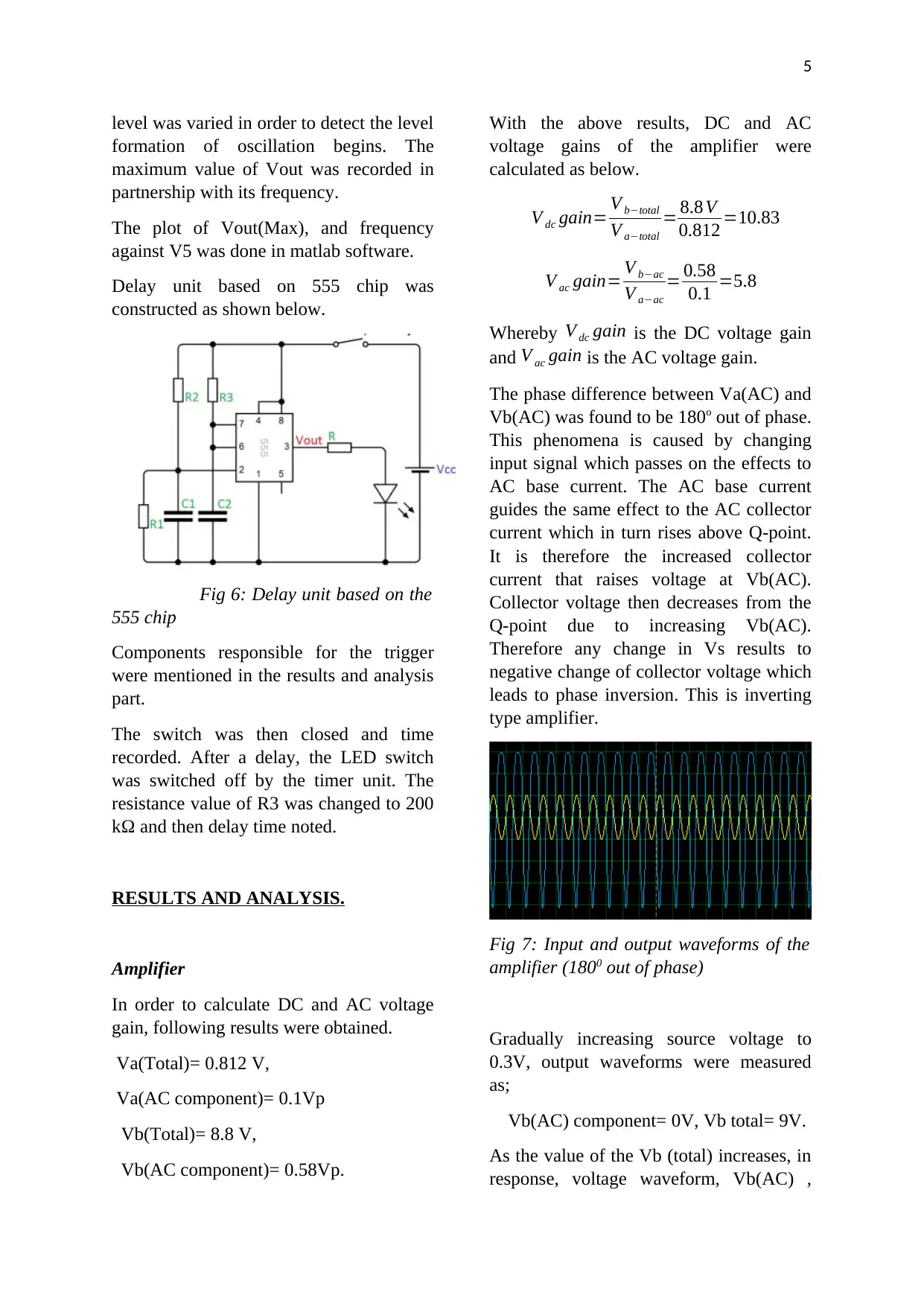
as shown in the figure 6.
External triggering signal for the time
delay circuit above changes with variation
of resistor R3 and Capacitor C2.
INTRODUCTION.
The project has dealt with pertinent issues
concerning practical implementation of the
electronic circuits. This report is divided
into four section with each section
designated a particular project task.
Modelling of the each assignment has been
outlined and results and analysis have been
tackled in the next section. Each model
was individually investigated and results
discussed in the next section.
SYSTEM MODEL
Designing of the amplifier.
The circuit as shown in figure 1 was
constructed on a breadboard. The values
R1=51kΩ, R2=5.1 kΩ, R3=1 kΩ, R4=82
kΩ, C=0.47μF and Vcc=9V. The source
voltage was set to a magnitude of 0.1V
with 1kHz frequency.
of four Nor gates. A multiple switching
between high and low value can be
realized with integration of logic gate
family. These logic gates are fundamental
blocks that gives characteristic output
depending on the input signal [4]. They
can be connected in tandem an oscillator
based Nor gate is as shown figure 2.
Design of oscillator and delay unit using
555chip
555 chip is an IC that is mostly used to
produce fine timing pulses. It operates in
three modes namely astable, monostable
and bistable. In astable mode of operation,
the output oscillates between low and high.
Therefore in astable mode, the 555 chip
can be used as clock to generate square
waves to execute many application.
However, in the monostable mode, the
user inputs an external state which is
displayed at the output. When the interrupt
subsides, the output goes automatically to
high since at this state it is unstable at low.
Finally, bistable mode have both outcomes
stable, either high or low. So, depending
on the type of interrupt, the output remains
in the initialized status until it receives
another interrupt [5].
A voltage controlled oscillator (VCO)
based IC 555 chip is basically used to
controlled frequency of the digital signal
using the voltage. The digital signal
waveform reciprocates repeatedly between
high and low state thus displaying a square
wave. By varying the input voltage, variety
of the frequencies can therefore be
obtained at the output pin of the oscillator
[6]. The output signal can be useful to
applications that need clocking system
such as processors. The circuit of voltage
controlled oscillator based on the IC 555
chip is as shown in figure 5.
Using IC 555 chip to fabricate a delay unit,
it can be operated in two modes namely a
monostable mode of operation and astable
mode of operation. The delay unit is said
to be in astable operation mode when pin 2
is connected to pin 6 thus self-triggering.
On the other hand, the delay unit is
considered to be in monostable operation
mode when the triggering elements are
externally located from the chip [7]. An
example of a monostable-type delay unit is
as shown in the figure 6.
External triggering signal for the time
delay circuit above changes with variation
of resistor R3 and Capacitor C2.
INTRODUCTION.
The project has dealt with pertinent issues
concerning practical implementation of the
electronic circuits. This report is divided
into four section with each section
designated a particular project task.
Modelling of the each assignment has been
outlined and results and analysis have been
tackled in the next section. Each model
was individually investigated and results
discussed in the next section.
SYSTEM MODEL
Designing of the amplifier.
The circuit as shown in figure 1 was
constructed on a breadboard. The values
R1=51kΩ, R2=5.1 kΩ, R3=1 kΩ, R4=82
kΩ, C=0.47μF and Vcc=9V. The source
voltage was set to a magnitude of 0.1V
with 1kHz frequency.
3
Fig 1: Common emitter transistor
amplifier.
AC and total voltages at node (a) and (b)
were determined using a digital multimeter
(DMM) and recorded simultaneously.
With values obtained above, it was
possible to calculate DC and AC voltage
gains of the transistor amplifier. The phase
different between AC components for
Va(AC) and Vb(AC) was also noted from
the equivalent signals in displayed the
oscilloscope.
Procedure for verifying input voltage
limitation to the output waveform was
conducted by resetting Vs gradually from
its initial value to 0.3V and concurrently
recording the output waveform Vb(Total)
and Vb(AC). In addition, the maximum
value of Vb(total) was deduced from the
oscilloscope.
Input frequency which is the factor that
directly influences output voltage was
proven experimentally by varying
frequency of Vs within a range of 10Hz
and 1MHz and noting the peak value of
Vb(AC). Values obtained were used to
determine the gain of the amplifier.
Furthermore, a plot of gain (A) against
frequency was plotted with help of Matlab
Software.
Designing of the oscillator based on Nor
gates.
The oscillator circuit was fabricated on the
breadboard as shown in the figure below.
Fig 2: Nor based oscillator
CD4001BCN chip was powered by
supplying Vcc=9V between Vcc pin (14)
and GND pin (7).
Waveforms at nodal points Va, Vb and Vc
were determined using the oscilloscope.
Besides waveforms, oscillating frequency
of the output waveform Vc was obtained
too.
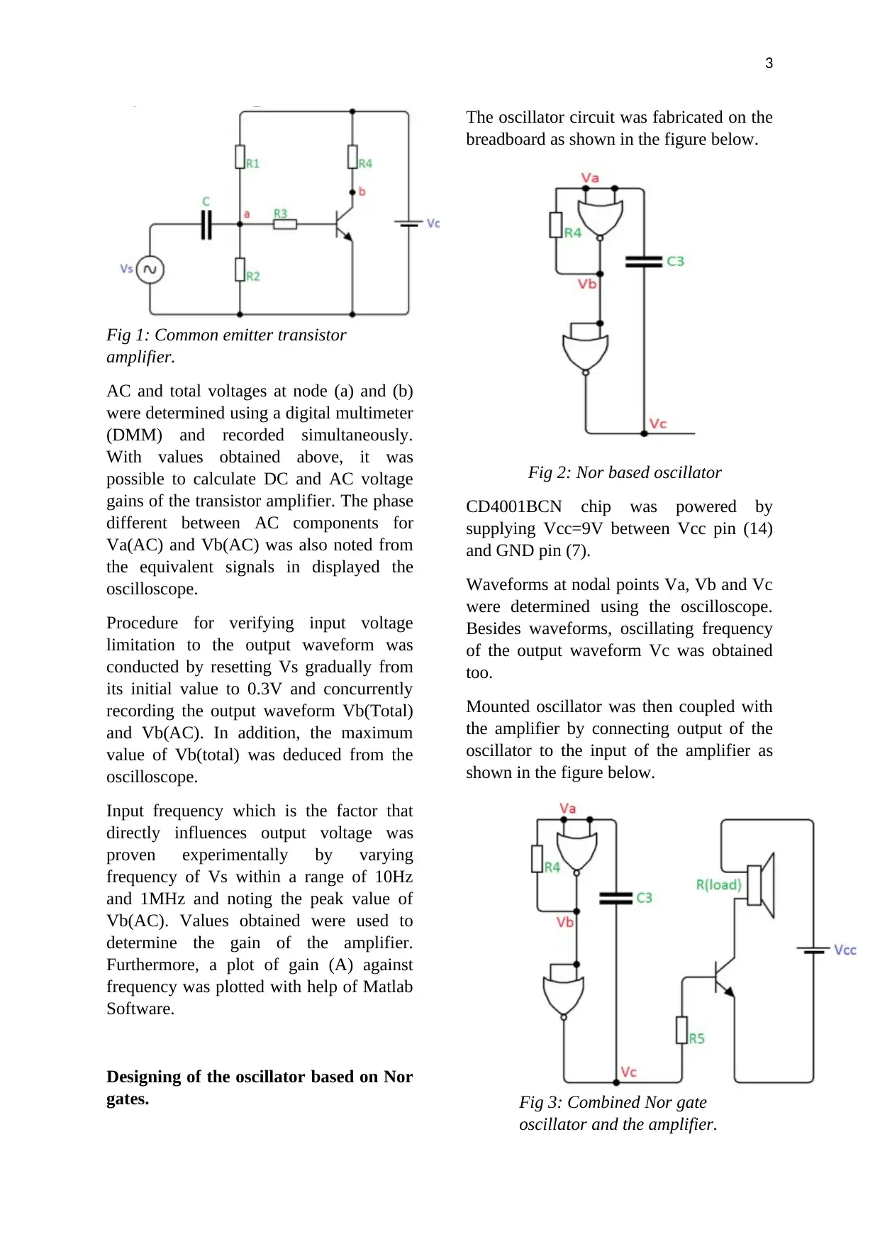
Mounted oscillator was then coupled with
the amplifier by connecting output of the
oscillator to the input of the amplifier as
shown in the figure below.
Fig 3: Combined Nor gate
oscillator and the amplifier.
Fig 1: Common emitter transistor
amplifier.
AC and total voltages at node (a) and (b)
were determined using a digital multimeter
(DMM) and recorded simultaneously.
With values obtained above, it was
possible to calculate DC and AC voltage
gains of the transistor amplifier. The phase
different between AC components for
Va(AC) and Vb(AC) was also noted from
the equivalent signals in displayed the
oscilloscope.
Procedure for verifying input voltage
limitation to the output waveform was
conducted by resetting Vs gradually from
its initial value to 0.3V and concurrently
recording the output waveform Vb(Total)
and Vb(AC). In addition, the maximum
value of Vb(total) was deduced from the
oscilloscope.
Input frequency which is the factor that
directly influences output voltage was
proven experimentally by varying
frequency of Vs within a range of 10Hz
and 1MHz and noting the peak value of
Vb(AC). Values obtained were used to
determine the gain of the amplifier.
Furthermore, a plot of gain (A) against
frequency was plotted with help of Matlab
Software.
Designing of the oscillator based on Nor
gates.
The oscillator circuit was fabricated on the
breadboard as shown in the figure below.
Fig 2: Nor based oscillator
CD4001BCN chip was powered by
supplying Vcc=9V between Vcc pin (14)
and GND pin (7).
Waveforms at nodal points Va, Vb and Vc
were determined using the oscilloscope.
Besides waveforms, oscillating frequency
of the output waveform Vc was obtained
too.
Mounted oscillator was then coupled with
the amplifier by connecting output of the
oscillator to the input of the amplifier as
shown in the figure below.
Fig 3: Combined Nor gate
oscillator and the amplifier.
4
(Note R5=100kΩ, R(load)=64Ω (which is
the loud speaker).
The sound was heard from the speaker the
moment connection was made.
Sound’s amplitude of the speaker was
investigated by reducing Vcc=9 stepwise
to 5.6V.
The circuit was reconstructed as shown
below. Values of the components are
R4=100k Ω, R7=1M Ω, R6=220k Ω,
C4=100nF. Impact of the change was
analyzed by investigating the quality of the
speaker’s sound.
Fig 4: Modified Nor
gate oscillator- amplifier circuit
Additional component was altered by
varying the value of R7 as 620kΩ-5.6M
Ω-10m Ω and then its effect was analyzed
by investigating quality of the sound from
the speaker.
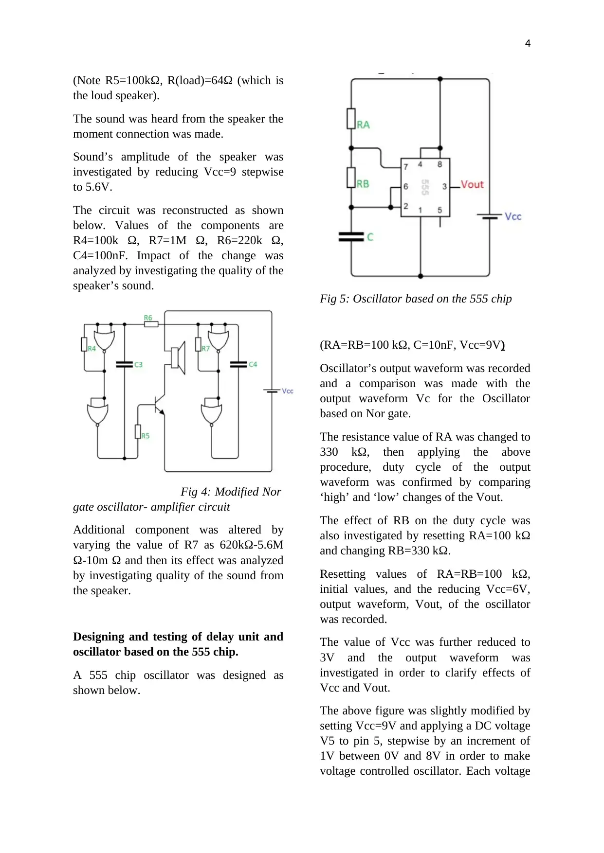
Designing and testing of delay unit and
oscillator based on the 555 chip.
A 555 chip oscillator was designed as
shown below.
Fig 5: Oscillator based on the 555 chip
(RA=RB=100 kΩ, C=10nF, Vcc=9V)
Oscillator’s output waveform was recorded
and a comparison was made with the
output waveform Vc for the Oscillator
based on Nor gate.
The resistance value of RA was changed to
330 kΩ, then applying the above
procedure, duty cycle of the output
waveform was confirmed by comparing
‘high’ and ‘low’ changes of the Vout.
The effect of RB on the duty cycle was
also investigated by resetting RA=100 kΩ
and changing RB=330 kΩ.
Resetting values of RA=RB=100 kΩ,
initial values, and the reducing Vcc=6V,
output waveform, Vout, of the oscillator
was recorded.
The value of Vcc was further reduced to
3V and the output waveform was
investigated in order to clarify effects of
Vcc and Vout.
The above figure was slightly modified by
setting Vcc=9V and applying a DC voltage
V5 to pin 5, stepwise by an increment of
1V between 0V and 8V in order to make
voltage controlled oscillator. Each voltage
(Note R5=100kΩ, R(load)=64Ω (which is
the loud speaker).
The sound was heard from the speaker the
moment connection was made.
Sound’s amplitude of the speaker was
investigated by reducing Vcc=9 stepwise
to 5.6V.
The circuit was reconstructed as shown
below. Values of the components are
R4=100k Ω, R7=1M Ω, R6=220k Ω,
C4=100nF. Impact of the change was
analyzed by investigating the quality of the
speaker’s sound.
Fig 4: Modified Nor
gate oscillator- amplifier circuit
Additional component was altered by
varying the value of R7 as 620kΩ-5.6M
Ω-10m Ω and then its effect was analyzed
by investigating quality of the sound from
the speaker.
Designing and testing of delay unit and
oscillator based on the 555 chip.
A 555 chip oscillator was designed as
shown below.
Fig 5: Oscillator based on the 555 chip
(RA=RB=100 kΩ, C=10nF, Vcc=9V)
Oscillator’s output waveform was recorded
and a comparison was made with the
output waveform Vc for the Oscillator
based on Nor gate.
The resistance value of RA was changed to
330 kΩ, then applying the above
procedure, duty cycle of the output
waveform was confirmed by comparing
‘high’ and ‘low’ changes of the Vout.
The effect of RB on the duty cycle was
also investigated by resetting RA=100 kΩ
and changing RB=330 kΩ.
Resetting values of RA=RB=100 kΩ,
initial values, and the reducing Vcc=6V,
output waveform, Vout, of the oscillator
was recorded.
The value of Vcc was further reduced to
3V and the output waveform was
investigated in order to clarify effects of
Vcc and Vout.
The above figure was slightly modified by
setting Vcc=9V and applying a DC voltage
V5 to pin 5, stepwise by an increment of
1V between 0V and 8V in order to make
voltage controlled oscillator. Each voltage
Secure Best Marks with AI Grader
Need help grading? Try our AI Grader for instant feedback on your assignments.
5
level was varied in order to detect the level
formation of oscillation begins. The
maximum value of Vout was recorded in
partnership with its frequency.
The plot of Vout(Max), and frequency
against V5 was done in matlab software.
Delay unit based on 555 chip was
constructed as shown below.
Fig 6: Delay unit based on the
555 chip
Components responsible for the trigger
were mentioned in the results and analysis
part.
The switch was then closed and time
recorded. After a delay, the LED switch
was switched off by the timer unit. The
resistance value of R3 was changed to 200
kΩ and then delay time noted.
RESULTS AND ANALYSIS.
Amplifier
In order to calculate DC and AC voltage
gain, following results were obtained.
Va(Total)= 0.812 V,
Va(AC component)= 0.1Vp
Vb(Total)= 8.8 V,
Vb(AC component)= 0.58Vp.
With the above results, DC and AC
voltage gains of the amplifier were
calculated as below.
V dc gain= V b−total
V a−total
= 8.8 V
0.812 =10.83
V ac gain= V b−ac
V a−ac
= 0.58
0.1 =5.8
Whereby V dc gain is the DC voltage gain
and V ac gain is the AC voltage gain.
The phase difference between Va(AC) and
Vb(AC) was found to be 180o out of phase.
This phenomena is caused by changing
input signal which passes on the effects to
AC base current. The AC base current
guides the same effect to the AC collector
current which in turn rises above Q-point.
It is therefore the increased collector
current that raises voltage at Vb(AC).
Collector voltage then decreases from the
Q-point due to increasing Vb(AC).
Therefore any change in Vs results to
negative change of collector voltage which
leads to phase inversion. This is inverting
type amplifier.
Fig 7: Input and output waveforms of the
amplifier (1800 out of phase)
Gradually increasing source voltage to
0.3V, output waveforms were measured
as;
Vb(AC) component= 0V, Vb total= 9V.
As the value of the Vb (total) increases, in
response, voltage waveform, Vb(AC) ,
6
also increases. On contrary, when the DC
component is eliminated, Vb(AC) is
measured as zero due to the transistor
lacking D.C biasing. Thus, the positive
wave component of Vb(AC) is clipped.
With the value of source voltage (Vs) reset
to 0.1V, the peak values of Vb(AC) were
recorded in partnership with the varying
frequency of Vs from 10Hz to 1MHz as
shown below;
Table 1: Values Obtained when frequency
of the Vs of the Amplifier was varied
Vs
frequency
Vb(AC) in
V
Voltage
gain (A)
10Hz 6.4 61
100Hz 6.8 68
1kHZ 8.8 68
10kHz 8.8 68
100kHz 8.8 68
Fig 8: Frequency against voltage
gain of the transistor amplifier
The transistor amplifier behaves like a
high pass filter whose cut-off frequency is
100Hz.
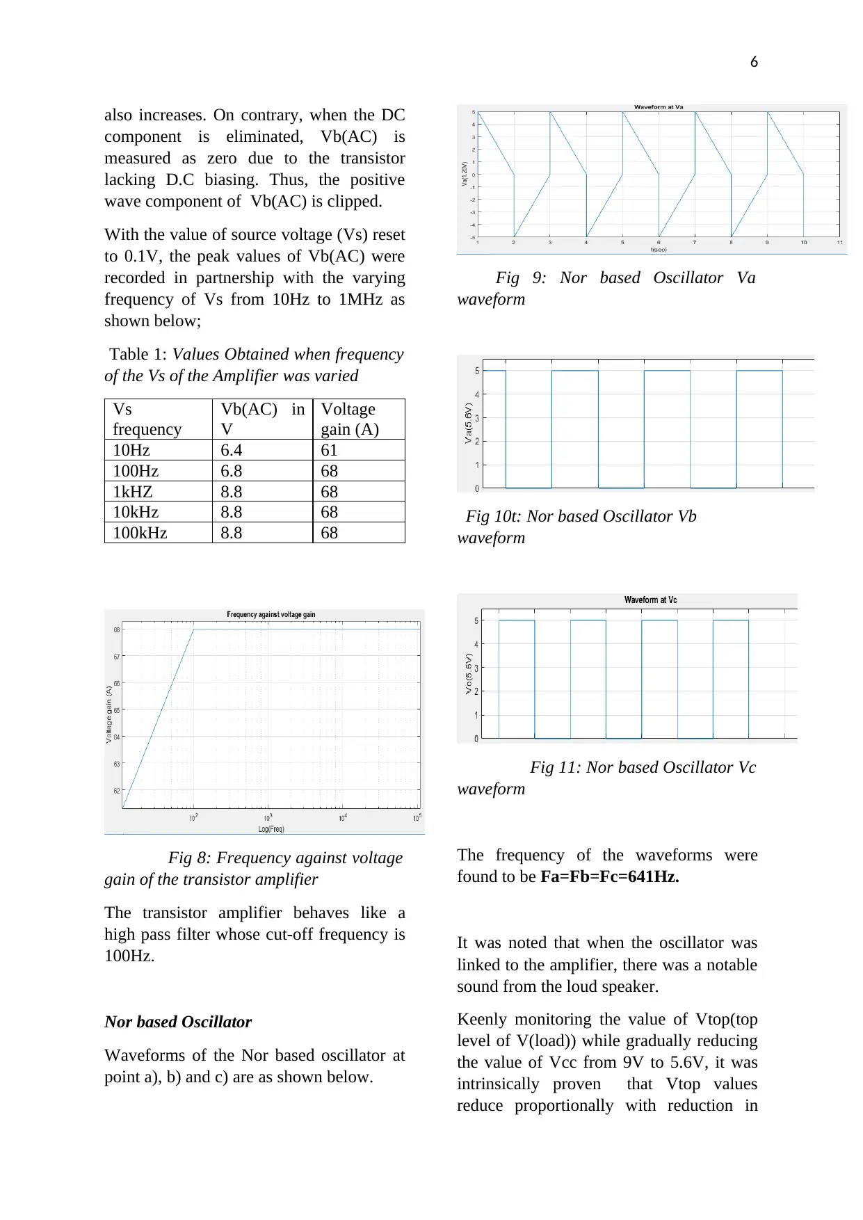
Nor based Oscillator
Waveforms of the Nor based oscillator at
point a), b) and c) are as shown below.
Fig 9: Nor based Oscillator Va
waveform
Fig 10t: Nor based Oscillator Vb
waveform
Fig 11: Nor based Oscillator Vc
waveform
The frequency of the waveforms were
found to be Fa=Fb=Fc=641Hz.
It was noted that when the oscillator was
linked to the amplifier, there was a notable
sound from the loud speaker.
Keenly monitoring the value of Vtop(top
level of V(load)) while gradually reducing
the value of Vcc from 9V to 5.6V, it was
intrinsically proven that Vtop values
reduce proportionally with reduction in
also increases. On contrary, when the DC
component is eliminated, Vb(AC) is
measured as zero due to the transistor
lacking D.C biasing. Thus, the positive
wave component of Vb(AC) is clipped.
With the value of source voltage (Vs) reset
to 0.1V, the peak values of Vb(AC) were
recorded in partnership with the varying
frequency of Vs from 10Hz to 1MHz as
shown below;
Table 1: Values Obtained when frequency
of the Vs of the Amplifier was varied
Vs
frequency
Vb(AC) in
V
Voltage
gain (A)
10Hz 6.4 61
100Hz 6.8 68
1kHZ 8.8 68
10kHz 8.8 68
100kHz 8.8 68
Fig 8: Frequency against voltage
gain of the transistor amplifier
The transistor amplifier behaves like a
high pass filter whose cut-off frequency is
100Hz.
Nor based Oscillator
Waveforms of the Nor based oscillator at
point a), b) and c) are as shown below.
Fig 9: Nor based Oscillator Va
waveform
Fig 10t: Nor based Oscillator Vb
waveform
Fig 11: Nor based Oscillator Vc
waveform
The frequency of the waveforms were
found to be Fa=Fb=Fc=641Hz.
It was noted that when the oscillator was
linked to the amplifier, there was a notable
sound from the loud speaker.
Keenly monitoring the value of Vtop(top
level of V(load)) while gradually reducing
the value of Vcc from 9V to 5.6V, it was
intrinsically proven that Vtop values
reduce proportionally with reduction in
7
Vcc. This scenario has fundamental
influence to the amplitude of the sound.
The amplitude of the sound gradually
reduced accordingly.
Resistance value of R4 was varied while
monitoring change in the value of Vc and
corresponding frequency. The resultant
frequencies waveforms when R4 was
varied is as shown in the table below.
Table 2: Values obtained when R4 of the
Nor based oscillator was varied
R4 Vc frequency
1kΩ 5.6V 36.66kHz
10kΩ 5.6V 5.37kHz
620kΩ 5.6V 107.3Hz
3.3MΩ 5.6V 21.7Hz
From the table, values of Vc are not
affected by altering values of R4.
However, the frequency of the wave
reduces drastically with increase in the
value of R4.
The quality of sound became finer and
sharper with increase in frequency, thus
frequency is a principle factor which
strives to improve the quality of the sound.
Addition on another Nor gate based
oscillator on the circuit made the loud
speaker’s sound to be of higher quality as
compared when only a single oscillator is
used.
The resultant values shown in the table
below are as a result of increasing the
value of R7 the
figure 4
Table 3: Values recorded when modified
Nor gate oscillator’s R7 was changed
R7 Vc Vout F(out) Fc
1
MΩ
5.6V 5.6V 708Hz 708Hz
5.6 5.6V 5.6V 726Hz 726Hz
MΩ
10
MΩ
5.6V 5.6V 728Hz 728Hz
The decision of using 64 Ω loud speaker
other than 8 Ω loud speaker was based on
the power it possesses. A 64 Ω loud
speaker has more power that 8 Ω resistor,
therefore, it can withstand the circuit
voltage used.
Results and analysis of IC 555 chip as an
oscillator and a unit delay.
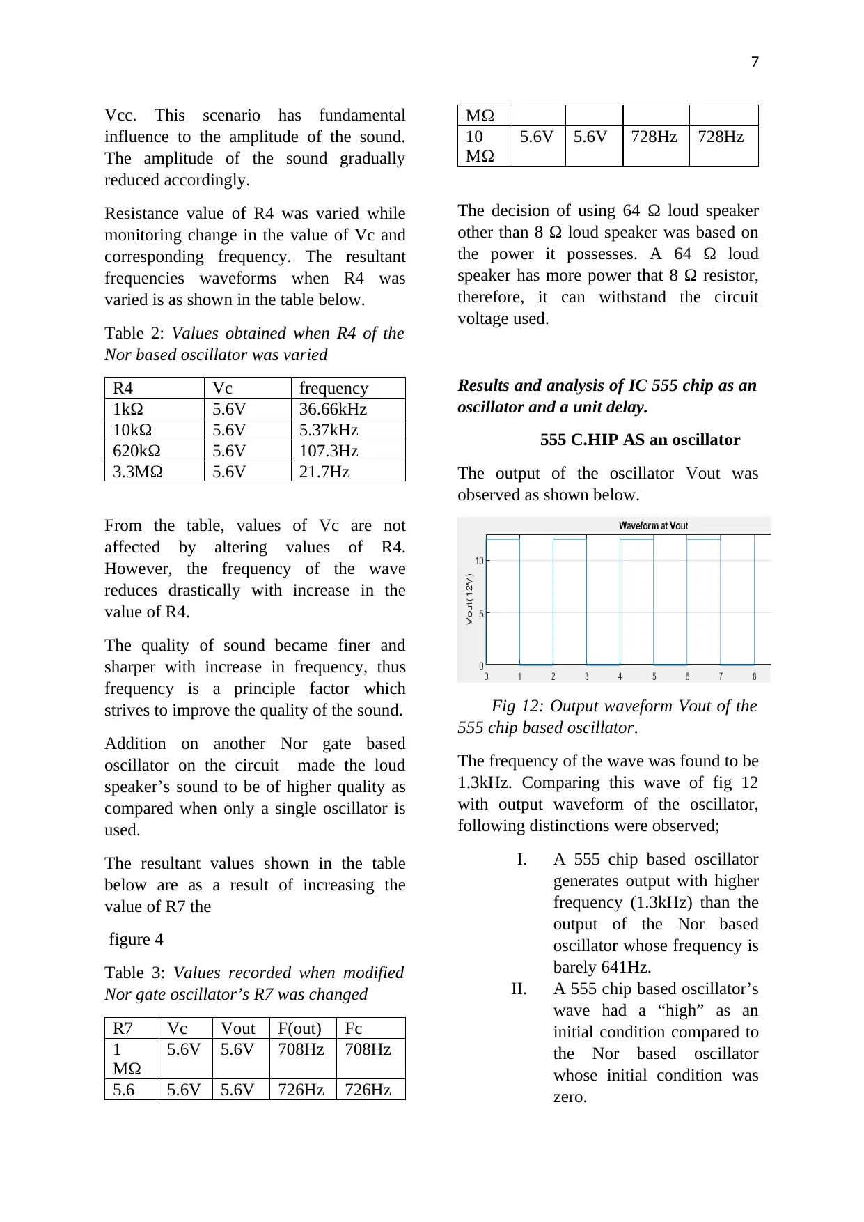
555 C.HIP AS an oscillator
The output of the oscillator Vout was
observed as shown below.
Fig 12: Output waveform Vout of the
555 chip based oscillator.
The frequency of the wave was found to be
1.3kHz. Comparing this wave of fig 12
with output waveform of the oscillator,
following distinctions were observed;
I. A 555 chip based oscillator
generates output with higher
frequency (1.3kHz) than the
output of the Nor based
oscillator whose frequency is
barely 641Hz.
II. A 555 chip based oscillator’s
wave had a “high” as an
initial condition compared to
the Nor based oscillator
whose initial condition was
zero.
Vcc. This scenario has fundamental
influence to the amplitude of the sound.
The amplitude of the sound gradually
reduced accordingly.
Resistance value of R4 was varied while
monitoring change in the value of Vc and
corresponding frequency. The resultant
frequencies waveforms when R4 was
varied is as shown in the table below.
Table 2: Values obtained when R4 of the
Nor based oscillator was varied
R4 Vc frequency
1kΩ 5.6V 36.66kHz
10kΩ 5.6V 5.37kHz
620kΩ 5.6V 107.3Hz
3.3MΩ 5.6V 21.7Hz
From the table, values of Vc are not
affected by altering values of R4.
However, the frequency of the wave
reduces drastically with increase in the
value of R4.
The quality of sound became finer and
sharper with increase in frequency, thus
frequency is a principle factor which
strives to improve the quality of the sound.
Addition on another Nor gate based
oscillator on the circuit made the loud
speaker’s sound to be of higher quality as
compared when only a single oscillator is
used.
The resultant values shown in the table
below are as a result of increasing the
value of R7 the
figure 4
Table 3: Values recorded when modified
Nor gate oscillator’s R7 was changed
R7 Vc Vout F(out) Fc
1
MΩ
5.6V 5.6V 708Hz 708Hz
5.6 5.6V 5.6V 726Hz 726Hz
MΩ
10
MΩ
5.6V 5.6V 728Hz 728Hz
The decision of using 64 Ω loud speaker
other than 8 Ω loud speaker was based on
the power it possesses. A 64 Ω loud
speaker has more power that 8 Ω resistor,
therefore, it can withstand the circuit
voltage used.
Results and analysis of IC 555 chip as an
oscillator and a unit delay.
555 C.HIP AS an oscillator
The output of the oscillator Vout was
observed as shown below.
Fig 12: Output waveform Vout of the
555 chip based oscillator.
The frequency of the wave was found to be
1.3kHz. Comparing this wave of fig 12
with output waveform of the oscillator,
following distinctions were observed;
I. A 555 chip based oscillator
generates output with higher
frequency (1.3kHz) than the
output of the Nor based
oscillator whose frequency is
barely 641Hz.
II. A 555 chip based oscillator’s
wave had a “high” as an
initial condition compared to
the Nor based oscillator
whose initial condition was
zero.
Paraphrase This Document
Need a fresh take? Get an instant paraphrase of this document with our AI Paraphraser
8
III. A 555 chip based oscillator
can operate at a slightly
higher voltage unlike a
similar case with Nor gate
based oscillator.
Increasing the RA to 330 kΩ, the
waveform of Vout was noted have a duty
cycle of 78%, as compared to the previous
waveform.
Fig 13: The Output waveform
Vout when RA=300 kΩ
The output waveform when RB is set at
330 kΩ and RA at 100 kΩ.
Fig 14: Output waveform Vout when
330 kΩ and RA at 100 kΩ
It is a square waveform whose duty cycle
is 50% as shown below.
Generally, the waveform of a 555 chip
based oscillator is different from the output
waveform of the Nor gate based oscillator.
This can be explained by the efficiency of
the 555 chip that can be triggered
electrically by applying triggering voltage
at pin 2. Also, 555 chip has an in-build
triggering components which can operate
at a higher triggering frequency.
With reduction of Vcc to 6V and
RA=RB=100 kΩ, the output waveform of
the oscillator is as shown below.
Fig 15 :Output waveform of the
oscillator with Vc=6V, and RA=RB=100
kΩ.
Peak voltage of the output has reduced
accordingly with reduction in Vcc. The
Duty cycle is 63%
At 3V Vcc the output waveform is as
shown below.
Fig 16: Output wave of the 555 chip
based oscillator when Vcc= 3 V and
RA=RB=100 kΩ.
From the analysis above, it can be
concluded that amplitude and duty cycle of
the output waveform varies with changing
input to the oscillator chip.
9
555 chip as a voltage controlled oscillator
(VCO).
Pin number 5 of the 555 chip controls
voltage output of the VCO by
manipulating the timing of the 555 and
overriding internal voltage divider
network. Therefore, this pin can be used to
the duty cycle of the output voltage signal
independent of the timing network of RC.
For the VCO connected, the smallest duty
cycle was 3.7%, at Vout=20mV and
Fc=150Hz at Vc=9V.
The maximum value of Vout achieved was
Vout=8.8 V at 8V and duty cycle is 81%.
When control voltage is low, the frequency
of the output voltage is high and when the
control signal is high, the output of the
control signal is low.
555 chip as a delay unit
Components which triggers unit delay
based on the 555 chip are Resistor R3 and
capacitor C2.
When the switch was pressed, the LED
lights for 12 sec and then automatically
switched off.
Doubling the resistance of R3 to 200kΩ in
return doubled time duration the delay unit
initiated OFF function by 24 sec.
The timer duration is directly proportional
to the value of resistance R3 and
capacitance C3. Therefore, if the delay
does not take 10 sec when R3 =100 kΩ,
the value of capacitor C2 can therein be
adjusted to fulfill the demand.
CONCLUSION.
Various electronic circuits have been dealt
with to a level of deeper understanding of
their properties and functionality.
Common emitter transistor amplifier have
been designed and practically
implemented. Much have been clarified
concerning amplifiers with practical
implementation to back-up theoretical
background. Furthermore, the design based
on the IC 555 chip has shown how
versatile electronic solid devices can be
used in many application to equally
perform indented purpose. The 555 IC
chip have been used to design timer,
oscillators and unit delay. For further
verification, oscillator based on Nor gate
chip have been implemented and results
compared with the other type.
10
REFERENCES
1. Charles John, (2018,
July).”Transistor Amplifier”.
Looking for Latest Project Kits.
Available:
http://www.circuitstoday.com/trans
istor-amplifier
2. Aspencore, Common emmiter
Amplifier [Online]: Available;
Electronics Tutorials,
https://www.electronics-
tutorials.ws/amplifier/amp_2.html
3. Pearson, “BJT Amplifier”,
[Online]: Available:
https://www.pearsonhighered.com/
assets/samplechapter/0/1/3/4/01344
20101.pdf
4. S. Kim, Lee, Chung, Park, Shin,
Choi, and Park (2009). “Single-
Electron-Based Flexible
Multivalued Exclusive-or Logic
gate”. IEEE Transactions on
Electron Devices, 56(5), 1048-
1055
5. Elprocus, ”Infographics: A brief
About IC 555 Timer And Its
Applications”, [Online]: Available:
Electronics| Project| Focus.
https://www.elprocus.com/brief-
about-ic-555-timer/
6. Xavier Richard, “Simple Time
Delay Circuit using 555 Timer”
Circuit Digest, [Online]: Available;
https://circuitdigest.com/electronic-
circuits/555-time-delay-circuit-
diagram
7. N. Tejeshwar,”A min project on
Dark Sensor using LC555 Timer”,
Dept, Electronics and
Communication Engineering,
Vaagdevi College of Engineering,
Delhi.
1 out of 10
Related Documents


Your All-in-One AI-Powered Toolkit for Academic Success.
+13062052269
info@desklib.com
Available 24*7 on WhatsApp / Email
![[object Object]](/_next/static/media/star-bottom.7253800d.svg)
Unlock your academic potential
© 2024 | Zucol Services PVT LTD | All rights reserved.