logo

Effect of Circuit Parameters on MOS and BJT Differential Amplifiers

Create a custom MOSFET differential pair circuit, using simulation to evaluate circuit behaviour, comparing results to hand calculations and investigating the impact of various circuit parameters.

3 Pages1486 Words297 Views
   

Added on  2023-03-31

About This Document

This report investigates the effect of variations in circuit parameters on MOS and BJT differential amplifiers. It explores the increase in amplifier gain with an increase in load resistance and the decrease in gain with the use of emitter degeneration resistances. The report includes findings from design, simulation, and practical implementation of the amplifiers.

Effect of Circuit Parameters on MOS and BJT Differential Amplifiers

Create a custom MOSFET differential pair circuit, using simulation to evaluate circuit behaviour, comparing results to hand calculations and investigating the impact of various circuit parameters.

   Added on 2023-03-31

ShareRelated Documents
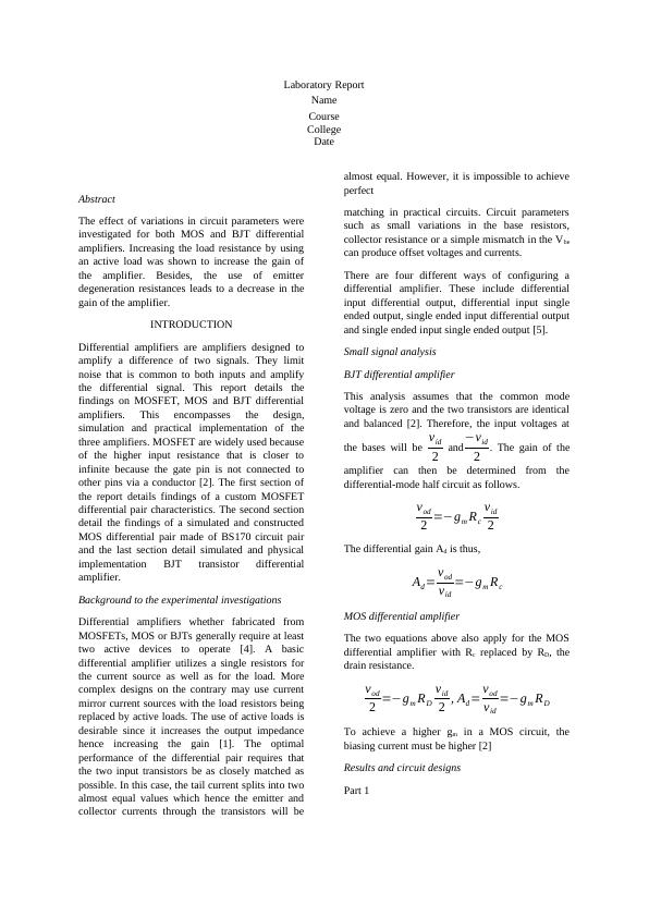
Laboratory Report
Name
Course
College
Date
Abstract
The effect of variations in circuit parameters were
investigated for both MOS and BJT differential
amplifiers. Increasing the load resistance by using
an active load was shown to increase the gain of
the amplifier. Besides, the use of emitter
degeneration resistances leads to a decrease in the
gain of the amplifier.
INTRODUCTION
Differential amplifiers are amplifiers designed to
amplify a difference of two signals. They limit
noise that is common to both inputs and amplify
the differential signal. This report details the
findings on MOSFET, MOS and BJT differential
amplifiers. This encompasses the design,
simulation and practical implementation of the
three amplifiers. MOSFET are widely used because
of the higher input resistance that is closer to
infinite because the gate pin is not connected to
other pins via a conductor [2]. The first section of
the report details findings of a custom MOSFET
differential pair characteristics. The second section
detail the findings of a simulated and constructed
MOS differential pair made of BS170 circuit pair
and the last section detail simulated and physical
implementation BJT transistor differential
amplifier.
Background to the experimental investigations
Differential amplifiers whether fabricated from
MOSFETs, MOS or BJTs generally require at least
two active devices to operate [4]. A basic
differential amplifier utilizes a single resistors for
the current source as well as for the load. More
complex designs on the contrary may use current
mirror current sources with the load resistors being
replaced by active loads. The use of active loads is
desirable since it increases the output impedance
hence increasing the gain [1]. The optimal
performance of the differential pair requires that
the two input transistors be as closely matched as
possible. In this case, the tail current splits into two
almost equal values which hence the emitter and
collector currents through the transistors will be
almost equal. However, it is impossible to achieve
perfect
matching in practical circuits. Circuit parameters
such as small variations in the base resistors,
collector resistance or a simple mismatch in the Vbe
can produce offset voltages and currents.
There are four different ways of configuring a
differential amplifier. These include differential
input differential output, differential input single
ended output, single ended input differential output
and single ended input single ended output [5].
Small signal analysis
BJT differential amplifier
This analysis assumes that the common mode
voltage is zero and the two transistors are identical
and balanced [2]. Therefore, the input voltages at
the bases will be vid
2 andvid
2 . The gain of the
amplifier can then be determined from the
differential-mode half circuit as follows.
vod
2 =gm Rc
vid
2
The differential gain Ad is thus,
Ad = vod
vid
=gm Rc
MOS differential amplifier
The two equations above also apply for the MOS
differential amplifier with Rc replaced by RD, the
drain resistance.
vod
2 =gm RD
vid
2 , Ad = vod
vid
=gm RD
To achieve a higher gm in a MOS circuit, the
biasing current must be higher [2]
Results and circuit designs
Part 1
Effect of Circuit Parameters on MOS and BJT Differential Amplifiers_1

End of preview

Want to access all the pages? Upload your documents or become a member.

Related Documents
Designing an Audio Amplifier: Steps and Analysis
|13
|2054
|268

Amplifier Circuits: Types, Characteristics and Applications
|19
|1241
|288

Principles and Applications of Electronic Devices and Circuits
|4
|1212
|69

Student. Professor. Principles and applications of Elec
|17
|1906
|56

Electronics engineering.
|14
|459
|45

Power Amplifiers Design and Simulation | Report
|27
|3863
|37